参数资料
| 型号: | A54SX08-1PQ208 |
| 厂商: | Microsemi SoC |
| 文件页数: | 64/64页 |
| 文件大小: | 0K |
| 描述: | IC FPGA SX 12K GATES 208-PQFP |
| 标准包装: | 24 |
| 系列: | SX |
| LAB/CLB数: | 768 |
| 输入/输出数: | 130 |
| 门数: | 12000 |
| 电源电压: | 3 V ~ 3.6 V,4.75 V ~ 5.25 V |
| 安装类型: | 表面贴装 |
| 工作温度: | 0°C ~ 70°C |
| 封装/外壳: | 208-BFQFP |
| 供应商设备封装: | 208-PQFP(28x28) |
第1页第2页第3页第4页第5页第6页第7页第8页第9页第10页第11页第12页第13页第14页第15页第16页第17页第18页第19页第20页第21页第22页第23页第24页第25页第26页第27页第28页第29页第30页第31页第32页第33页第34页第35页第36页第37页第38页第39页第40页第41页第42页第43页第44页第45页第46页第47页第48页第49页第50页第51页第52页第53页第54页第55页第56页第57页第58页第59页第60页第61页第62页第63页当前第64页
SX Family FPGAs
v3.2
1-5
DirectConnect is a horizontal routing resource that
provides connections from a C-cell to its neighboring R-
cell in a given SuperCluster. DirectConnect uses a
hardwired signal path requiring no programmable
interconnection to achieve its fast signal propagation
time of less than 0.1 ns.
FastConnect enables horizontal routing between any
two logic modules within a given SuperCluster and
vertical routing with the SuperCluster immediately
below it. Only one programmable connection is used in a
FastConnect
path,
delivering
maximum
pin-to-pin
propagation of 0.4 ns.
In addition to DirectConnect and FastConnect, the
architecture makes use of two globally oriented routing
resources known as segmented routing and high-drive
routing. The Actel segmented routing structure provides
a variety of track lengths for extremely fast routing
between SuperClusters. The exact combination of track
lengths and antifuses within each path is chosen by the
100 percent automatic place-and-route software to
minimize signal propagation delays.
The Actel high-drive routing structure provides three
clock networks. The first clock, called HCLK, is hardwired
from the HCLK buffer to the clock select multiplexer
(MUX) in each R-cell. This provides a fast propagation
path for the clock signal, enabling the 3.7 ns clock-to-out
(pin-to-pin)
performance
of
the
SX
devices.
The
hardwired clock is tuned to provide clock skew as low as
0.25 ns. The remaining two clocks (CLKA, CLKB) are
global clocks that can be sourced from external pins or
from internal logic signals within the SX device.
Other Architectural Features
Technology
The Actel SX family is implemented on a high-voltage
twin-well CMOS process using 0.35 design rules. The
metal-to-metal antifuse is made up of a combination of
amorphous silicon and dielectric material with barrier
metals and has a programmed ("on" state) resistance of
25
Ω with a capacitance of 1.0 fF for low signal impedance.
Performance
The combination of architectural features described
above enables SX devices to operate with internal clock
frequencies exceeding 300 MHz, enabling very fast
execution of even complex logic functions. Thus, the SX
family is an optimal platform upon which to integrate
the functionality previously contained in multiple CPLDs.
In addition, designs that previously would have required
a gate array to meet performance goals can now be
integrated
into
an
SX
device
with
dramatic
improvements in cost and time to market. Using timing-
driven place-and-route tools, designers can achieve
highly
deterministic
device
performance.
With
SX
devices, designers do not need to use complicated
performance-enhancing design techniques such as the
use of redundant logic to reduce fanout on critical nets
or the instantiation of macros in HDL code to achieve
high performance.
I/O Modules
Each I/O on an SX device can be configured as an input,
an output, a tristate output, or a bidirectional pin.
Even without the inclusion of dedicated I/O registers,
these I/Os, in combination with array registers, can
achieve clock-to-out (pad-to-pad) timing as fast as 3.7 ns.
I/O cells that have embedded latches and flip-flops
require instantiation in HDL code; this is a design
complication not encountered in SX FPGAs. Fast pin-to-
pin timing ensures that the device will have little trouble
interfacing with any other device in the system, which in
turn enables parallel design of system components and
reduces overall design time.
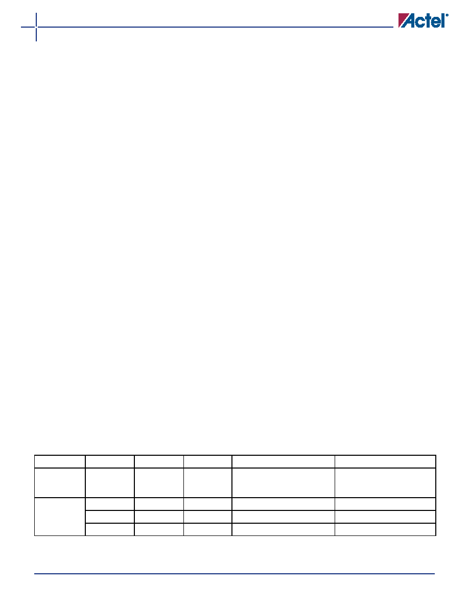
Power Requirements
The SX family supports 3.3 V operation and is designed
to tolerate 5.0 V inputs. (Table 1-1). Power consumption
is extremely low due to the very short distances signals
are required to travel to complete a circuit. Power
requirements are further reduced because of the small
number of low-resistance antifuses in the path. The
antifuse architecture does not require active circuitry to
hold a charge (as do SRAM or EPROM), making it the
lowest power architecture on the market.
Table 1-1
Supply Voltages
Device
VCCA
VCCI
VCCR
Maximum Input Tolerance
Maximum Output Drive
A54SX08
A54SX16
A54SX32
3.3 V
5.0 V
3.3 V
A54SX16-P*
3.3 V
5.0 V
3.3 V
5.0 V
Note: *A54SX16-P has three different entries because it is capable of both a 3.3 V and a 5.0 V drive.
相关PDF资料 |
PDF描述 |
|---|---|
| M7A3P1000-2FGG484 | IC FPGA 1KB FLASH 1M 484-FBGA |
| RBB100DHBN | CONN EDGECARD 200PS R/A .050 DIP |
| RBB100DHBD | CONN EDGECARD 200PS R/A .050 DIP |
| GMC65DRXN | CONN EDGECARD 130PS DIP .100 SLD |
| GMC65DRXH | CONN EDGECARD 130PS DIP .100 SLD |
相关代理商/技术参数 |
参数描述 |
|---|---|
| A54SX08-1PQ208I | 功能描述:IC FPGA SX 12K GATES 208-PQFP RoHS:否 类别:集成电路 (IC) >> 嵌入式 - FPGA(现场可编程门阵列) 系列:SX 标准包装:40 系列:SX-A LAB/CLB数:6036 逻辑元件/单元数:- RAM 位总计:- 输入/输出数:360 门数:108000 电源电压:2.25 V ~ 5.25 V 安装类型:表面贴装 工作温度:0°C ~ 70°C 封装/外壳:484-BGA 供应商设备封装:484-FPBGA(27X27) |
| A54SX08-1PQ208M | 制造商:未知厂家 制造商全称:未知厂家 功能描述:54SX Family FPGAs |
| A54SX08-1PQ208PP | 制造商:未知厂家 制造商全称:未知厂家 功能描述:54SX Family FPGAs |
| A54SX08-1PQG208 | 功能描述:IC FPGA SX 12K GATES 208-PQFP RoHS:是 类别:集成电路 (IC) >> 嵌入式 - FPGA(现场可编程门阵列) 系列:SX 标准包装:40 系列:SX-A LAB/CLB数:6036 逻辑元件/单元数:- RAM 位总计:- 输入/输出数:360 门数:108000 电源电压:2.25 V ~ 5.25 V 安装类型:表面贴装 工作温度:0°C ~ 70°C 封装/外壳:484-BGA 供应商设备封装:484-FPBGA(27X27) |
| A54SX08-1PQG208I | 功能描述:IC FPGA SX 12K GATES 208-PQFP RoHS:是 类别:集成电路 (IC) >> 嵌入式 - FPGA(现场可编程门阵列) 系列:SX 标准包装:40 系列:SX-A LAB/CLB数:6036 逻辑元件/单元数:- RAM 位总计:- 输入/输出数:360 门数:108000 电源电压:2.25 V ~ 5.25 V 安装类型:表面贴装 工作温度:0°C ~ 70°C 封装/外壳:484-BGA 供应商设备封装:484-FPBGA(27X27) |
发布紧急采购,3分钟左右您将得到回复。