参数资料
| 型号: | A54SX08-PL84 |
| 厂商: | Microsemi SoC |
| 文件页数: | 14/64页 |
| 文件大小: | 0K |
| 描述: | IC FPGA SX 12K GATES 84-PLCC |
| 标准包装: | 16 |
| 系列: | SX |
| LAB/CLB数: | 768 |
| 输入/输出数: | 69 |
| 门数: | 12000 |
| 电源电压: | 3 V ~ 3.6 V,4.75 V ~ 5.25 V |
| 安装类型: | 表面贴装 |
| 工作温度: | 0°C ~ 70°C |
| 封装/外壳: | 84-LCC(J 形引线) |
| 供应商设备封装: | 84-PLCC(29.31x29.31) |
第1页第2页第3页第4页第5页第6页第7页第8页第9页第10页第11页第12页第13页当前第14页第15页第16页第17页第18页第19页第20页第21页第22页第23页第24页第25页第26页第27页第28页第29页第30页第31页第32页第33页第34页第35页第36页第37页第38页第39页第40页第41页第42页第43页第44页第45页第46页第47页第48页第49页第50页第51页第52页第53页第54页第55页第56页第57页第58页第59页第60页第61页第62页第63页第64页
SX Family FPGAs
v3.2
1-17
shows
capacitance
values
for
various
devices.
Guidelines for Calculating Power
Consumption
The power consumption guidelines are meant to
represent worst-case scenarios so that they can be
generally used to predict the upper limits of power
dissipation. These guidelines are shown in Table 1-14.
Sample Power Calculation
One of the designs used to characterize the SX family
was a 528 bit serial-in, serial-out shift register. The design
utilized 100 percent of the dedicated flip-flops of an
A54SX16P device. A pattern of 0101… was clocked into
the device at frequencies ranging from 1 MHz to
200 MHz. Shifting in a series of 0101… caused 50 percent
of the flip-flops to toggle from low to high at every clock
cycle.
Follow the steps below to estimate power consumption.
The values provided for the sample calculation below are
for the shift register design above. This method for
estimating power consumption is conservative and the
actual power consumption of your design may be less
than the estimated power consumption.
The total power dissipation for the SX family is the sum
of the AC power dissipation and the DC power
dissipation.
PTotal = PAC (dynamic power) + PDC (static power)
EQ 1-9
AC Power Dissipation
PAC = PModule + PRCLKA Net + PRCLKB Net + PHCLK Net +
POutput Buffer + PInput Buffer
EQ 1-10
PAC = VCCA
2 × [(m × C
EQM × fm)Module +
(n × CEQI × fn)Input Buffer+ (p × (CEQO + CL) × fp)Output Buffer +
(0.5 (q1 × CEQCR × fq1) + (r1 × fq1))RCLKA +
(0.5 (q2 × CEQCR × fq2)+ (r2 × fq2))RCLKB +
(0.5 (s1 × CEQHV × fs1) + (CEQHF × fs1))HCLK]
EQ 1-11
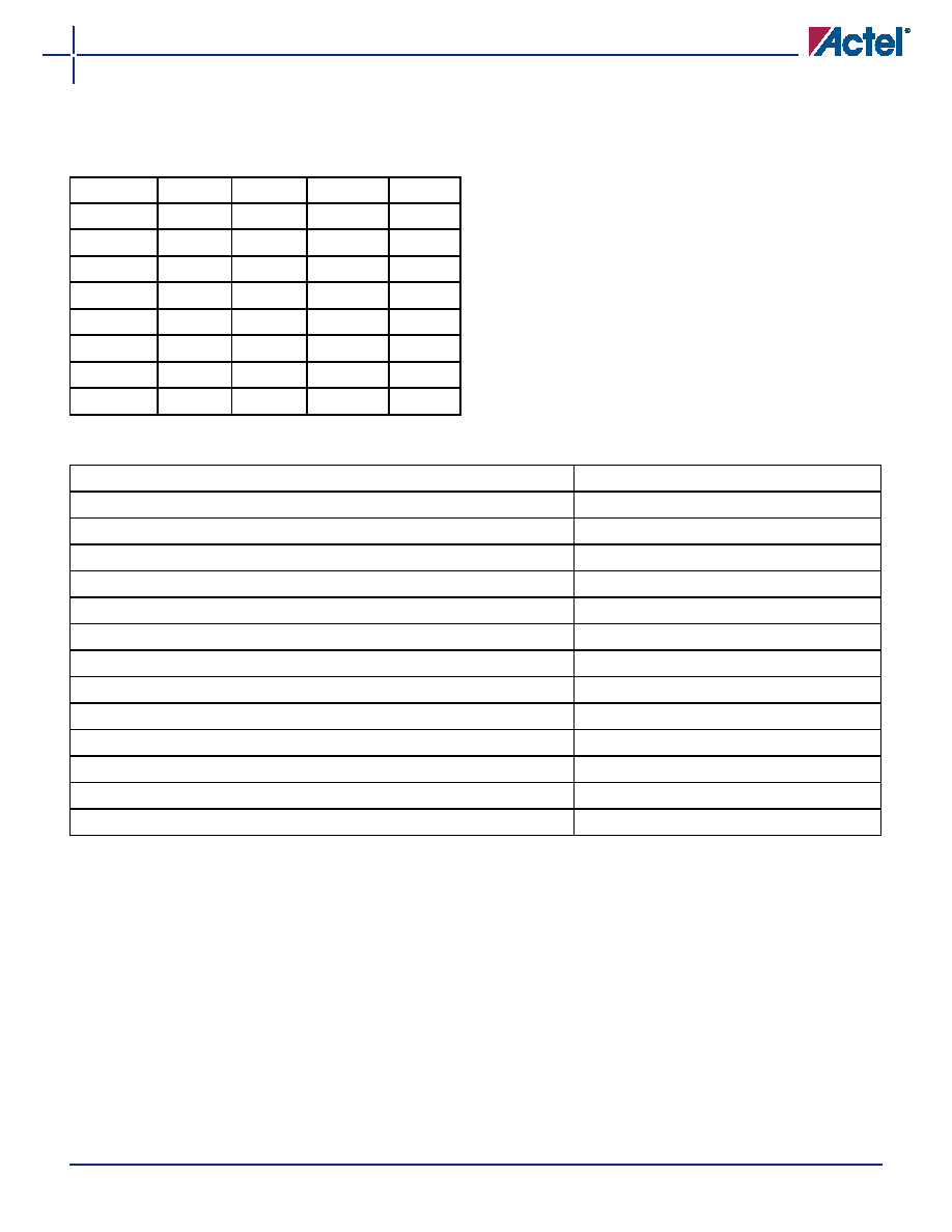
Table 1-13 Capacitance Values for Devices
A54SX08
A54SX16
A54SX16P A54SX32
CEQM (pF)
4.0
CEQI (pF)
3.4
CEQO (pF)
4.7
CEQCR (pF)
1.6
CEQHV
0.615
CEQHF
60
96
140
r1 (pF)
87
138
171
r2 (pF)
87
138
171
Table 1-14 Power Consumption Guidelines
Description
Power Consumption Guideline
Logic Modules (m)
20% of modules
Inputs Switching (n)
# inputs/4
Outputs Switching (p)
# outputs/4
First Routed Array Clock Loads (q1)
20% of register cells
Second Routed Array Clock Loads (q2)
20% of register cells
Load Capacitance (CL)
35 pF
Average Logic Module Switching Rate (fm)
f/10
Average Input Switching Rate (fn)
f/5
Average Output Switching Rate (fp)
f/10
Average First Routed Array Clock Rate (fq1)
f/2
Average Second Routed Array Clock Rate (fq2)
f/2
Average Dedicated Array Clock Rate (fs1)
f
Dedicated Clock Array Clock Loads (s1)
20% of regular modules
相关PDF资料 |
PDF描述 |
|---|---|
| M1AFS250-1QNG180I | IC FPGA 2MB FLASH 250K 180-QFN |
| RMA44DTMT | CONN EDGECARD 88POS R/A .125 SLD |
| IDT7130SA100P | IC SRAM 8KBIT 100NS 48DIP |
| RSA44DTBT | CONN EDGECARD 88POS R/A .125 SLD |
| IDT71V424L15PHG | IC SRAM 4MBIT 15NS 44TSOP |
相关代理商/技术参数 |
参数描述 |
|---|---|
| A54SX08-PL84I | 功能描述:IC FPGA SX 12K GATES 84-PLCC RoHS:否 类别:集成电路 (IC) >> 嵌入式 - FPGA(现场可编程门阵列) 系列:SX 标准包装:40 系列:SX-A LAB/CLB数:6036 逻辑元件/单元数:- RAM 位总计:- 输入/输出数:360 门数:108000 电源电压:2.25 V ~ 5.25 V 安装类型:表面贴装 工作温度:0°C ~ 70°C 封装/外壳:484-BGA 供应商设备封装:484-FPBGA(27X27) |
| A54SX08-PL84M | 制造商:未知厂家 制造商全称:未知厂家 功能描述:Field Programmable Gate Array (FPGA) |
| A54SX08-PLG84 | 功能描述:IC FPGA SX 12K GATES 84-PLCC RoHS:是 类别:集成电路 (IC) >> 嵌入式 - FPGA(现场可编程门阵列) 系列:SX 标准包装:90 系列:ProASIC3 LAB/CLB数:- 逻辑元件/单元数:- RAM 位总计:36864 输入/输出数:157 门数:250000 电源电压:1.425 V ~ 1.575 V 安装类型:表面贴装 工作温度:-40°C ~ 125°C 封装/外壳:256-LBGA 供应商设备封装:256-FPBGA(17x17) |
| A54SX08-PLG84I | 功能描述:IC FPGA SX 12K GATES 84-PLCC RoHS:是 类别:集成电路 (IC) >> 嵌入式 - FPGA(现场可编程门阵列) 系列:SX 标准包装:40 系列:SX-A LAB/CLB数:6036 逻辑元件/单元数:- RAM 位总计:- 输入/输出数:360 门数:108000 电源电压:2.25 V ~ 5.25 V 安装类型:表面贴装 工作温度:0°C ~ 70°C 封装/外壳:484-BGA 供应商设备封装:484-FPBGA(27X27) |
| A54SX08P-PL208 | 制造商:未知厂家 制造商全称:未知厂家 功能描述:54SX Family FPGAs |
发布紧急采购,3分钟左右您将得到回复。