参数资料
| 型号: | A54SX08A-FG144A |
| 厂商: | Microsemi SoC |
| 文件页数: | 26/108页 |
| 文件大小: | 0K |
| 描述: | IC FPGA SX 12K GATES 144-FBGA |
| 标准包装: | 160 |
| 系列: | SX-A |
| LAB/CLB数: | 768 |
| 输入/输出数: | 111 |
| 门数: | 12000 |
| 电源电压: | 2.25 V ~ 5.25 V |
| 安装类型: | 表面贴装 |
| 工作温度: | -40°C ~ 125°C |
| 封装/外壳: | 144-LBGA |
| 供应商设备封装: | 144-FPBGA(13x13) |
第1页第2页第3页第4页第5页第6页第7页第8页第9页第10页第11页第12页第13页第14页第15页第16页第17页第18页第19页第20页第21页第22页第23页第24页第25页当前第26页第27页第28页第29页第30页第31页第32页第33页第34页第35页第36页第37页第38页第39页第40页第41页第42页第43页第44页第45页第46页第47页第48页第49页第50页第51页第52页第53页第54页第55页第56页第57页第58页第59页第60页第61页第62页第63页第64页第65页第66页第67页第68页第69页第70页第71页第72页第73页第74页第75页第76页第77页第78页第79页第80页第81页第82页第83页第84页第85页第86页第87页第88页第89页第90页第91页第92页第93页第94页第95页第96页第97页第98页第99页第100页第101页第102页第103页第104页第105页第106页第107页第108页
SX-A Family FPGAs
2- 4
v5.3
Table 2-8 AC Specifications (5 V PCI Operation)
Symbol
Parameter
Condition
Min.
Max.
Units
IOH(AC)
Switching Current High
0 < VOUT ≤ 1.4
1
–44
–
mA
1.4
≤ V
OUT < 2.4
1, 2
(–44 + (VOUT – 1.4)/0.024)
–
mA
3.1 < VOUT < VCCI
1, 3
–
–
(Test Point)
VOUT = 3.1
3
––142
mA
IOL(AC)
Switching Current Low
VOUT ≥ 2.2
1
95
–
mA
2.2 > VOUT > 0.55
1
(VOUT/0.023)
–
mA
0.71 > VOUT > 0
1, 3
–
–
(Test Point)
VOUT = 0.71
3
–
206
mA
ICL
Low Clamp Current
–5 < VIN ≤ –1
–25 + (VIN + 1)/0.015
–
mA
slewR
Output Rise Slew Rate
0.4 V to 2.4 V load 4
15
V/ns
slewF
Output Fall Slew Rate
2.4 V to 0.4 V load 4
15
V/ns
Notes:
1. Refer to the V/I curves in Figure 2-1 on page 2-5. Switching current characteristics for REQ# and GNT# are permitted to be one half
of that specified here; i.e., half size output drivers may be used on these signals. This specification does not apply to CLK and RST#,
which are system outputs. “Switching Current High” specifications are not relevant to SERR#, INTA#, INTB#, INTC#, and INTD#,
which are open drain outputs.
2. Note that this segment of the minimum current curve is drawn from the AC drive point directly to the DC drive point rather than
toward the voltage rail (as is done in the pull-down curve). This difference is intended to allow for an optional N-channel pull-up.
3. Maximum current requirements must be met as drivers pull beyond the last step voltage. Equations defining these maximums (A
and B) are provided with the respective diagrams in Figure 2-1 on page 2-5. The equation defined maximum should be met by
design. In order to facilitate component testing, a maximum current test point is defined for each side of the output driver.
4. This parameter is to be interpreted as the cumulative edge rate across the specified range, rather than the instantaneous rate at any
point within the transition range. The specified load (diagram below) is optional; i.e., the designer may elect to meet this parameter
with an unloaded output per revision 2.0 of the PCI Local Bus Specification. However, adherence to both maximum and minimum
parameters is now required (the maximum is no longer simply a guideline). Since adherence to the maximum slew rate was not
required prior to revision 2.1 of the specification, there may be components in the market for some time that have faster edge
rates; therefore, motherboard designers must bear in mind that rise and fall times faster than this specification could occur and
should ensure that signal integrity modeling accounts for this. Rise slew rate does not apply to open drain outputs.
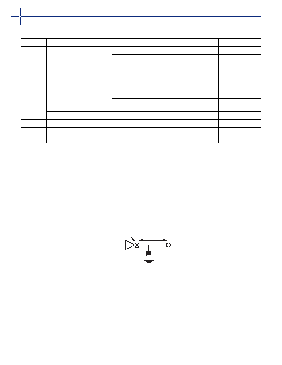
Output
Buffer
1/2 in. max.
50 pF
Pin
相关PDF资料 |
PDF描述 |
|---|---|
| A54SX08A-FGG144A | IC FPGA SX 12K GATES 144-FBGA |
| IDT71V424S10YG8 | IC SRAM 4MBIT 10NS 36SOJ |
| A54SX16A-PQG208A | IC FPGA SX 24K GATES 208-PQFP |
| A54SX16A-PQ208A | IC FPGA SX 24K GATES 208-PQFP |
| A3PE600-1FG256 | IC FPGA 600000 GATES 256-FBGA |
相关代理商/技术参数 |
参数描述 |
|---|---|
| A54SX08AFG144I | 制造商:未知厂家 制造商全称:未知厂家 功能描述:Logic IC |
| A54SX08A-FG144I | 功能描述:IC FPGA SX 12K GATES 144-FBGA RoHS:否 类别:集成电路 (IC) >> 嵌入式 - FPGA(现场可编程门阵列) 系列:SX-A 标准包装:90 系列:ProASIC3 LAB/CLB数:- 逻辑元件/单元数:- RAM 位总计:36864 输入/输出数:157 门数:250000 电源电压:1.425 V ~ 1.575 V 安装类型:表面贴装 工作温度:-40°C ~ 125°C 封装/外壳:256-LBGA 供应商设备封装:256-FPBGA(17x17) |
| A54SX08AFG144M | 制造商:未知厂家 制造商全称:未知厂家 功能描述:Logic IC |
| A54SX08A-FG208 | 制造商:未知厂家 制造商全称:未知厂家 功能描述:SX-A Family FPGAs |
| A54SX08AFG208A | 制造商:ACTEL 制造商全称:Actel Corporation 功能描述:SX-A Family FPGAs |
发布紧急采购,3分钟左右您将得到回复。