参数资料
| 型号: | A54SX32A-TQ176I |
| 厂商: | Microsemi SoC |
| 文件页数: | 13/108页 |
| 文件大小: | 0K |
| 描述: | IC FPGA SX 48K GATES 176-TQFP |
| 标准包装: | 40 |
| 系列: | SX-A |
| LAB/CLB数: | 2880 |
| 输入/输出数: | 147 |
| 门数: | 48000 |
| 电源电压: | 2.25 V ~ 5.25 V |
| 安装类型: | 表面贴装 |
| 工作温度: | -40°C ~ 85°C |
| 封装/外壳: | 176-LQFP |
| 供应商设备封装: | 176-TQFP(24x24) |
第1页第2页第3页第4页第5页第6页第7页第8页第9页第10页第11页第12页当前第13页第14页第15页第16页第17页第18页第19页第20页第21页第22页第23页第24页第25页第26页第27页第28页第29页第30页第31页第32页第33页第34页第35页第36页第37页第38页第39页第40页第41页第42页第43页第44页第45页第46页第47页第48页第49页第50页第51页第52页第53页第54页第55页第56页第57页第58页第59页第60页第61页第62页第63页第64页第65页第66页第67页第68页第69页第70页第71页第72页第73页第74页第75页第76页第77页第78页第79页第80页第81页第82页第83页第84页第85页第86页第87页第88页第89页第90页第91页第92页第93页第94页第95页第96页第97页第98页第99页第100页第101页第102页第103页第104页第105页第106页第107页第108页
SX-A Family FPGAs
1- 8
v5.3
Power-Up/Down and Hot Swapping
SX-A I/Os are configured to be hot-swappable, with the
exception of 3.3 V PCI. During power-up/down (or partial
up/down), all I/Os are tristated. VCCA and VCCI do not
have to be stable during power-up/down, and can be
powered up/down in any order. When the SX-A device is
plugged into an electrically active system, the device will
not degrade the reliability of or cause damage to the
host system. The device’s output pins are driven to a high
impedance state until normal chip operating conditions
which the I/Os behave according to the user’s design for
an SX-A device at room temperature for various ramp-up
rates. The data reported assumes a linear ramp-up
profile to 2.5 V. For more information on power-up and
hot-swapping, refer to the application note, Actel SX-A
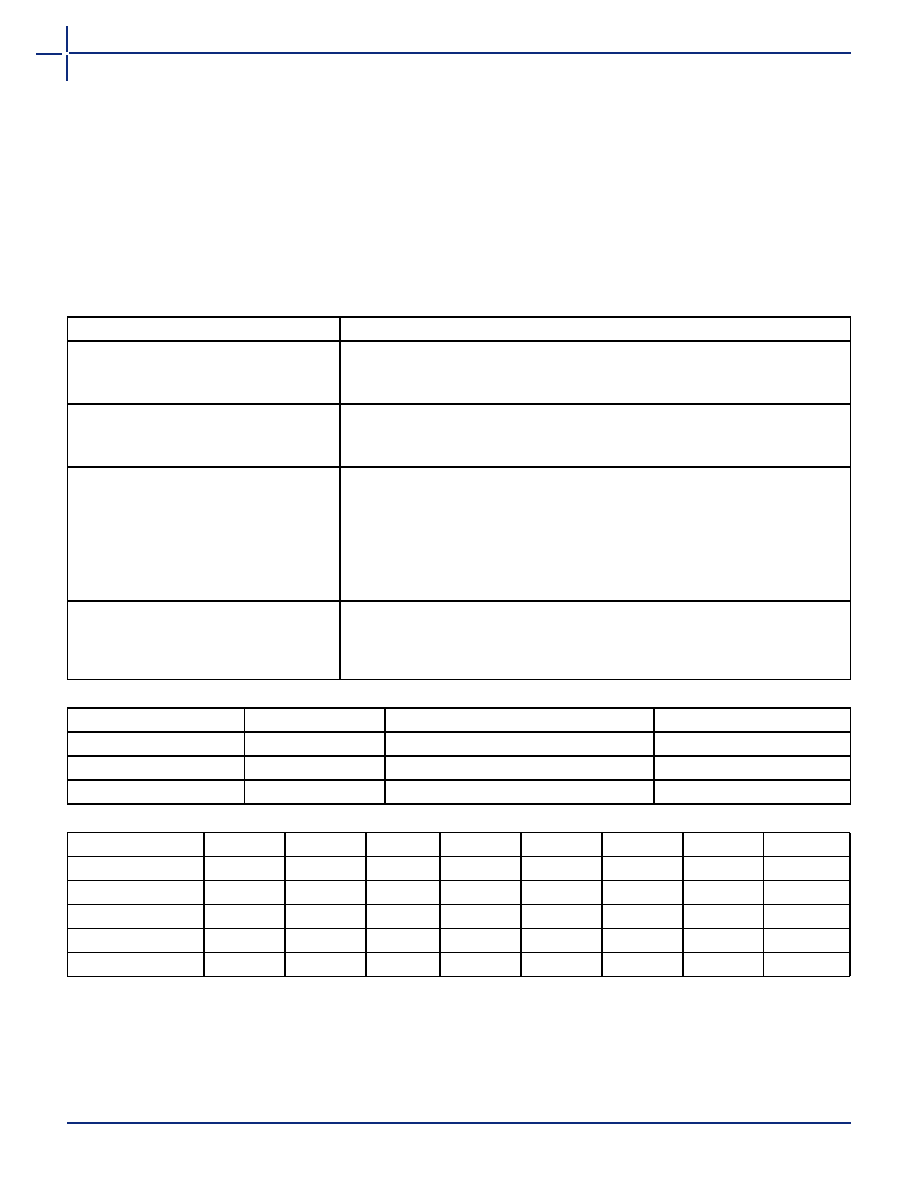
Table 1-2 I/O Features
Function
Description
Input Buffer Threshold Selections
5 V: PCI, TTL
3.3 V: PCI, LVTTL
2.5 V: LVCMOS2 (commercial only)
Flexible Output Driver
5 V: PCI, TTL
3.3 V: PCI, LVTTL
2.5 V: LVCMOS2 (commercial only)
Output Buffer
“Hot-Swap” Capability (3.3 V PCI is not hot swappable)
I/O on an unpowered device does not sink current
Can be used for “cold-sparing”
Selectable on an individual I/O basis
Individually selectable slew rate; high slew or low slew (The default is high slew rate).
The slew is only affected on the falling edge of an output. Rising edges of outputs are
not affected.
Power-Up
Individually selectable pull-ups and pull-downs during power-up (default is to power-up
in tristate)
Enables deterministic power-up of device
VCCA and VCCI can be powered in any order
Table 1-3 I/O Characteristics for All I/O Configurations
Hot Swappable
Slew Rate Control
Power-Up Resistor
TTL, LVTTL, LVCMOS2
Yes
Yes. Only affects falling edges of outputs
Pull-up or pull-down
3.3 V PCI
No
No. High slew rate only
Pull-up or pull-down
5 V PCI
Yes
No. High slew rate only
Pull-up or pull-down
Table 1-4 Power-Up Time at which I/Os Become Active
Supply Ramp Rate
0.25 V/
μs 0.025 V/μs
5 V/ms
2.5 V/ms
0.5 V/ms
0.25 V/ms
0.1 V/ms
0.025 V/ms
Units
μs
ms
msms
ms
A54SX08A
10
96
0.34
0.65
2.7
5.4
12.9
50.8
A54SX16A
10
100
0.36
0.62
2.5
4.7
11.0
41.6
A54SX32A
10
100
0.46
0.74
2.8
5.2
12.1
47.2
A54SX72A
10
100
0.41
0.67
2.6
5.0
12.1
47.2
相关PDF资料 |
PDF描述 |
|---|---|
| AGM40DRSD | CONN EDGECARD 80POS DIP .156 SLD |
| HSC44DRYS-S93 | CONN EDGECARD 88POS DIP .100 SLD |
| EEC43DTEI | CONN EDGECARD 86POS .100 EYELET |
| ASC49DRTN | CONN EDGECARD 98POS .100 DIP SLD |
| ASC49DRTH | CONN EDGECARD 98POS .100 DIP SLD |
相关代理商/技术参数 |
参数描述 |
|---|---|
| A54SX32A-TQ176M | 制造商:Microsemi Corporation 功能描述:FPGA SX-A 32K GATES 1800 CELLS 238MHZ 0.25UM/0.22UM 2.5V 176 - Trays 制造商:Microsemi Corporation 功能描述:IC FPGA 147 I/O 176TQFP 制造商:Microsemi Corporation 功能描述:IC FPGA 48K GATES 176TQFP |
| A54SX32A-TQG100 | 功能描述:IC FPGA 249I/O 100TQFP RoHS:是 类别:集成电路 (IC) >> 嵌入式 - FPGA(现场可编程门阵列) 系列:SX-A 标准包装:24 系列:ECP2 LAB/CLB数:1500 逻辑元件/单元数:12000 RAM 位总计:226304 输入/输出数:131 门数:- 电源电压:1.14 V ~ 1.26 V 安装类型:表面贴装 工作温度:0°C ~ 85°C 封装/外壳:208-BFQFP 供应商设备封装:208-PQFP(28x28) |
| A54SX32A-TQG100A | 功能描述:IC FPGA SX 48K GATES 100-TQFP RoHS:是 类别:集成电路 (IC) >> 嵌入式 - FPGA(现场可编程门阵列) 系列:SX-A 标准包装:40 系列:SX-A LAB/CLB数:6036 逻辑元件/单元数:- RAM 位总计:- 输入/输出数:360 门数:108000 电源电压:2.25 V ~ 5.25 V 安装类型:表面贴装 工作温度:0°C ~ 70°C 封装/外壳:484-BGA 供应商设备封装:484-FPBGA(27X27) |
| A54SX32A-TQG100I | 功能描述:IC FPGA SX 48K GATES 100-TQFP RoHS:是 类别:集成电路 (IC) >> 嵌入式 - FPGA(现场可编程门阵列) 系列:SX-A 标准包装:40 系列:SX-A LAB/CLB数:6036 逻辑元件/单元数:- RAM 位总计:- 输入/输出数:360 门数:108000 电源电压:2.25 V ~ 5.25 V 安装类型:表面贴装 工作温度:0°C ~ 70°C 封装/外壳:484-BGA 供应商设备封装:484-FPBGA(27X27) |
| A54SX32A-TQG100M | 制造商:Microsemi Corporation 功能描述:FPGA SX-A Family 32K Gates 1800 Cells 238MHz 0.25um Technology 2.5V 100-Pin TQFP 制造商:Microsemi Corporation 功能描述:FPGA SX-A 32K GATES 1800 CELLS 238MHZ 0.25UM/0.22UM 2.5V 100 - Trays |
发布紧急采购,3分钟左右您将得到回复。