参数资料
| 型号: | A54SX72A-FG484A |
| 厂商: | Microsemi SoC |
| 文件页数: | 14/108页 |
| 文件大小: | 0K |
| 描述: | IC FPGA SX-A 108K 484-FBGA |
| 标准包装: | 40 |
| 系列: | SX-A |
| LAB/CLB数: | 6036 |
| 输入/输出数: | 360 |
| 门数: | 108000 |
| 电源电压: | 2.25 V ~ 5.25 V |
| 安装类型: | 表面贴装 |
| 工作温度: | -40°C ~ 125°C |
| 封装/外壳: | 484-BGA |
| 供应商设备封装: | 484-FPBGA(27X27) |
第1页第2页第3页第4页第5页第6页第7页第8页第9页第10页第11页第12页第13页当前第14页第15页第16页第17页第18页第19页第20页第21页第22页第23页第24页第25页第26页第27页第28页第29页第30页第31页第32页第33页第34页第35页第36页第37页第38页第39页第40页第41页第42页第43页第44页第45页第46页第47页第48页第49页第50页第51页第52页第53页第54页第55页第56页第57页第58页第59页第60页第61页第62页第63页第64页第65页第66页第67页第68页第69页第70页第71页第72页第73页第74页第75页第76页第77页第78页第79页第80页第81页第82页第83页第84页第85页第86页第87页第88页第89页第90页第91页第92页第93页第94页第95页第96页第97页第98页第99页第100页第101页第102页第103页第104页第105页第106页第107页第108页
SX-A Family FPGAs
v5.3
1-9
Boundary-Scan Testing (BST)
All SX-A devices are IEEE 1149.1 compliant and offer
superior diagnostic and testing capabilities by providing
Boundary Scan Testing (BST) and probing capabilities.
The BST function is controlled through the special JTAG
pins (TMS, TDI, TCK, TDO, and TRST). The functionality of
the JTAG pins is defined by two available modes:
Dedicated and Flexible. TMS cannot be employed as a
user I/O in either mode.
Dedicated Mode
In Dedicated mode, all JTAG pins are reserved for BST;
designers cannot use them as regular I/Os. An internal
pull-up resistor is automatically enabled on both TMS
and TDI pins, and the TMS pin will function as defined in
the IEEE 1149.1 (JTAG) specification.
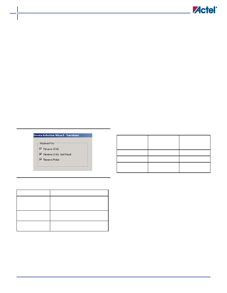
To select Dedicated mode, the user must reserve the
JTAG pins in Actel’s Designer software. Reserve the JTAG
pins by checking the Reserve JTAG box in the Device
Selection Wizard (Figure 1-12).
The default for the software is Flexible mode; all boxes
are unchecked. Table 1-5 lists the definitions of the
options in the Device Selection Wizard.
Flexible Mode
In Flexible mode, TDI, TCK, and TDO may be employed as
either user I/Os or as JTAG input pins. The internal
resistors on the TMS and TDI pins are not present in
flexible JTAG mode.
To select the Flexible mode, uncheck the Reserve JTAG
box in the Device Selection Wizard dialog in the Actel
Designer software. In Flexible mode, TDI, TCK, and TDO
pins may function as user I/Os or BST pins. The
functionality is controlled by the BST Test Access Port
(TAP) controller. The TAP controller receives two control
inputs, TMS and TCK. Upon power-up, the TAP controller
enters the Test-Logic-Reset state. In this state, TDI, TCK,
and TDO function as user I/Os. The TDI, TCK, and TDO are
transformed from user I/Os into BST pins when a rising
edge on TCK is detected while TMS is at logic low. To
return to Test-Logic Reset state, TMS must be high for at
least five TCK cycles. An external 10 k pull-up resistor
to VCCI should be placed on the TMS pin to pull it
High by default.
describes
the
different
configuration
requirements of BST pins and their functionality in
different modes.
TRST Pin
The TRST pin functions as a dedicated Boundary-Scan
Reset pin when the Reserve JTAG Test Reset option is
selected as shown in Figure 1-12. An internal pull-up
resistor is permanently enabled on the TRST pin in this
mode. Actel recommends connecting this pin to ground
in normal operation to keep the JTAG state controller in
the Test-Logic-Reset state. When JTAG is being used, it
can be left floating or can be driven high.
When the Reserve JTAG Test Reset option is not
selected, this pin will function as a regular I/O. If unused
as an I/O in the design, it will be configured as a tristated
output.
Figure 1-12 Device Selection Wizard
Table 1-5 Reserve Pin Definitions
Pin
Function
Reserve JTAG
Keeps pins from being used and
changes the behavior of JTAG pins (no
pull-up on TMS)
Reserve
JTAG
Test
Reset
Regular I/O or JTAG reset with an
internal pull-up
Reserve Probe
Keeps pins from being used or regular
I/O
Table 1-6 Boundary-Scan Pin Configurations and
Functions
Mode
Designer
"Reserve JTAG"
Selection
TAP Controller
State
Dedicated (JTAG)
Checked
Any
Flexible (User I/O)
Unchecked
Test-Logic-Reset
Flexible (JTAG)
Unchecked
Any EXCEPT Test-
Logic-Reset
相关PDF资料 |
PDF描述 |
|---|---|
| AGLE600V2-FG484I | IC FPGA 1KB FLASH 600K 484-FBGA |
| AGLE600V2-FGG484I | IC FPGA 1KB FLASH 600K 484-FBGA |
| EP4CGX50DF27I7 | IC CYCLONE IV GX FPGA 50K 672FBG |
| EP4CGX50DF27C6 | IC CYCLONE IV GX FPGA 50K 672FBG |
| 93C46C-I/P | IC EEPROM 1KBIT 3MHZ 8DIP |
相关代理商/技术参数 |
参数描述 |
|---|---|
| A54SX72A-FG484I | 功能描述:IC FPGA SX-A 108K 484-FBGA RoHS:否 类别:集成电路 (IC) >> 嵌入式 - FPGA(现场可编程门阵列) 系列:SX-A 产品培训模块:Three Reasons to Use FPGA's in Industrial Designs Cyclone IV FPGA Family Overview 特色产品:Cyclone? IV FPGAs 标准包装:60 系列:CYCLONE® IV GX LAB/CLB数:9360 逻辑元件/单元数:149760 RAM 位总计:6635520 输入/输出数:270 门数:- 电源电压:1.16 V ~ 1.24 V 安装类型:表面贴装 工作温度:0°C ~ 85°C 封装/外壳:484-BGA 供应商设备封装:484-FBGA(23x23) |
| A54SX72A-FG484M | 制造商:Microsemi Corporation 功能描述:FPGA SX-A Family 72K Gates 4024 Cells 217MHz 0.25um Technology 2.5V 484-Pin FBGA 制造商:Microsemi Corporation 功能描述:FPGA SX-A Family 72K Gates 4024 Cells 217MHz 0.25um/0.22um (CMOS) Technology 2.5V 484-Pin FBGA 制造商:Microsemi Corporation 功能描述:FPGA SX-A 72K GATES 4024 CELLS 217MHZ 0.25UM/0.22UM 2.5V 484 - Trays |
| A54SX72A-FGG256 | 功能描述:IC FPGA SX-A 108K 256-FBGA RoHS:是 类别:集成电路 (IC) >> 嵌入式 - FPGA(现场可编程门阵列) 系列:SX-A 产品培训模块:Three Reasons to Use FPGA's in Industrial Designs Cyclone IV FPGA Family Overview 特色产品:Cyclone? IV FPGAs 标准包装:60 系列:CYCLONE® IV GX LAB/CLB数:9360 逻辑元件/单元数:149760 RAM 位总计:6635520 输入/输出数:270 门数:- 电源电压:1.16 V ~ 1.24 V 安装类型:表面贴装 工作温度:0°C ~ 85°C 封装/外壳:484-BGA 供应商设备封装:484-FBGA(23x23) |
| A54SX72A-FGG256A | 功能描述:IC FPGA SX-A 108K 256-FBGA RoHS:是 类别:集成电路 (IC) >> 嵌入式 - FPGA(现场可编程门阵列) 系列:SX-A 产品培训模块:Three Reasons to Use FPGA's in Industrial Designs Cyclone IV FPGA Family Overview 特色产品:Cyclone? IV FPGAs 标准包装:60 系列:CYCLONE® IV GX LAB/CLB数:9360 逻辑元件/单元数:149760 RAM 位总计:6635520 输入/输出数:270 门数:- 电源电压:1.16 V ~ 1.24 V 安装类型:表面贴装 工作温度:0°C ~ 85°C 封装/外壳:484-BGA 供应商设备封装:484-FBGA(23x23) |
| A54SX72A-FGG256I | 功能描述:IC FPGA SX-A 108K 256-FBGA RoHS:是 类别:集成电路 (IC) >> 嵌入式 - FPGA(现场可编程门阵列) 系列:SX-A 产品培训模块:Three Reasons to Use FPGA's in Industrial Designs Cyclone IV FPGA Family Overview 特色产品:Cyclone? IV FPGAs 标准包装:60 系列:CYCLONE® IV GX LAB/CLB数:9360 逻辑元件/单元数:149760 RAM 位总计:6635520 输入/输出数:270 门数:- 电源电压:1.16 V ~ 1.24 V 安装类型:表面贴装 工作温度:0°C ~ 85°C 封装/外壳:484-BGA 供应商设备封装:484-FBGA(23x23) |
发布紧急采购,3分钟左右您将得到回复。