- 您现在的位置:买卖IC网 > PDF目录1774 > A8287SLBTR (Allegro Microsystems Inc)IC REG LNB SUPPLY/CTRL 24-SOIC PDF资料下载
参数资料
| 型号: | A8287SLBTR |
| 厂商: | Allegro Microsystems Inc |
| 文件页数: | 10/18页 |
| 文件大小: | 0K |
| 描述: | IC REG LNB SUPPLY/CTRL 24-SOIC |
| 标准包装: | 1,000 |
| 应用: | 转换器,模拟和数字式卫星信号接收器 |
| 输入电压: | 9 V ~ 16 V |
| 输出数: | 1 |
| 输出电压: | 12.7 V ~ 20.4 V |
| 工作温度: | -20°C ~ 85°C |
| 安装类型: | 表面贴装 |
| 封装/外壳: | 24-SOIC(0.295",7.50mm 宽) |
| 供应商设备封装: | 24-SOIC W |
| 包装: | 带卷 (TR) |
�� �
�
�A8285� and�
�A8287�
�LNB� Supply� and� Control� Voltage� Regulator�
�SDA� line� before� the� ninth� clock� cycle,� in� order� to� allow� this�
�handshaking� to� occur.�
�During� a� data� read,� the� A8285/A8287� acknowledges� the� address�
�in� the� same� way� as� in� the� data� write� sequence,� and� then� retains�
�control� of� the� SDA� line� and� send� the� data� to� the� master.� On�
�completion� of� the� eight� data� bits,� the� A8285/A8287� releases�
�the� SDA� line� before� the� ninth� clock� cycle,� in� order� to� allow� the�
�master� to� acknowledge� the� data.� If� the� master� holds� the� SDA� line�
�low� during� this� Acknowledge� bit,� the� A8285/A8287� responds� by�
�sending� another� data� byte� to� the� master.� Data� bytes� continue� to� be�
�sent� to� the� master� until� the� master� releases� the� SDA� line� during�
�the� Acknowledge� bit.� When� this� is� detected,� the� A8285/A8287�
�stops� sending� data� and� waits� for� a� stop� signal.�
�Interrupt� Request� .� The� A8285/A8287� also� provides� an� inter-�
�rupt� request� pin� IRQ,� which� is� an� open-drain,� active-low� output.�
�This� output� may� be� connected� to� a� common� IRQ� line� with� a�
�suitable� external� pull-up� and� can� be� used� with� other� I� 2� C� devices�
�to� request� attention� from� the� master� controller.� The� IRQ� output�
�becomes� active� when� either� the� A8285/A8287� first� recognizes� a�
�fault� condition,� or� at� power-on� when� the� main� supply� V� IN� and� the�
�internal� logic� supply� V� REG� reach� the� correct� operating� condi-�
�tions.� It� is� only� reset� to� inactive� when� the� I� 2� C� master� addresses�
�the� A8285/A8287� with� the� Read/Write� bit� set� (causing� a� read).�
�Fault� conditions� are� indicated� by� the� TSD,� VUV,� and� OCP� bits�
�in� the� status� register� (see� description� of� OCP� for� conditions� of�
�use).� The� DIS� and� PNG� bits� do� not� cause� an� interrupt.� When� the�
�master� recognizes� an� interrupt,� it� addresses� all� slaves� connected�
�to� the� interrupt� line� in� sequence,� and� then� reads� the� status� register�
�to� determine� which� device� is� requesting� attention.� The� A8285/�
�A8287� latches� all� conditions� in� the� status� register� until� the�
�completion� of� the� data� read.�
�The� action� at� the� resampling� point� is� further� defined� in� the�
�description� for� each� of� the� status� bits.� The� bits� in� the� status� reg-�
�Reading� the� Register� After� an� Interrupt�
�ister� are� defined� such� that� the� all-zero� condition� indicates� that� the�
�A8285/A8287� is� fully� active� with� no� fault� conditions.�
�When� V� IN� is� initially� applied,� the� I� 2� C� interface� does� not� respond�
�to� any� requests� until� the� internal� logic� supply� V� REG� has� reached�
�its� operating� level.� Once� V� REG� has� reached� this� point,� the� IRQ�
�output� goes� active,� and� the� VUV� bit� is� set.� After� the� A8285/�
�A8287� acknowledges� the� address,� the� IRQ� flag� is� reset.� Once� the�
�master� reads� the� status� registers,� the� registers� are� updated� with�
�the� VUV� reset.�
�Control� Register� (Write� Register).� All� main� functions� of� the�
�A8285/A8287� are� controlled� through� the� I� 2� C� interface� via� the�
�8-bit� Control� register.� This� register� allows� selection� of� the� output�
�voltage� and� current� limit,� enabling� and� disabling� the� LNB� output,�
�and� switching� the� 22� kHz� tone� on� and� off.� The� power-up� state� is� 0�
�for� all� of� the� control� functions.�
�Bit� 0� (VSEL0),� Bit� 1� (VSEL1),� and� Bit� 2� (VSEL2)� .� These�
�provide� incremental� control� over� the� voltage� on� the� LNB� output.�
�The� available� voltages� provide� the� necessary� levels� for� all� the�
�common� standards� plus� the� ability� to� add� line� compensation� in�
�increments� of� 333� mV.� The� voltage� levels� are� defined� in� the� Out-�
�put� Voltage� Amplitude� Selection� table.�
�Bit� 3� (VSEL3)� .� Switches� between� the� low-level� and� high-level�
�output� voltages� on� the� LNB� output.� A� value� of� 0� selects� the� low�
�level� voltage� and� a� value� of� 1� selects� the� high� level.� The� low-�
�level� center� voltage� is� 12.709� V� nominal,� and� the� high� level� is�
�18.042� V� nominal.� These� may� be� increased,� in� increments� of� 333�
�mV,� by� using� the� VSEL2,� VSEL1,� and� VSEL0� control� register�
�bits.�
�Bit� 4� (ODT)� .� When� set� to� 1,� enables� the� ODT� feature� (disables�
�the� A8285/A8287� if� the� overcurrent� disable� time� is� exceeded�
�during� an� overcurrent� condition� on� the� output).� When� set� to� 0,� the�
�ODT� feature� is� disabled.�
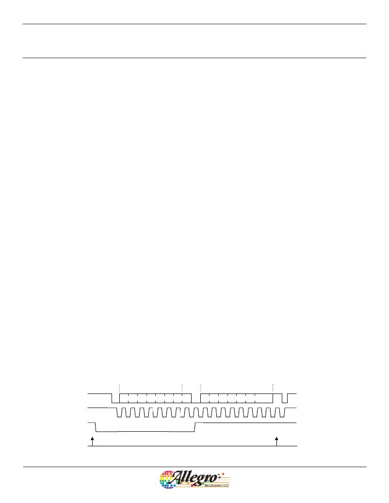
�Start�
�Address�
�R�
�Status� Data�
�Stop�
�SDA�
�0�
�0�
�0�
�1�
�0�
�A1�
�A0�
�1�
�AK�
�D7�
�D6�
�D5�
�D4�
�D3�
�D2�
�D1�
�D0� NAK�
�SCL�
�1�
�2�
�3�
�4�
�5�
�6�
�7�
�8�
�9�
�IRQ�
�Fault�
�Event�
�Reload�
�Status� Register�
�Allegro� MicroSystems,� LLC�
�115� Northeast� Cutoff�
�Worcester,� Massachusetts� 01615-0036� U.S.A.�
�1.508.853.5000;� www.allegromicro.com�
�10�
�相关PDF资料 |
PDF描述 |
|---|---|
| A8290SETTR-T | IC VOLTAGE REG SGL LNB 28-QFN |
| A8291SETTR-T | IC VOLTAGE REG SGL LNB 28-QFN |
| A8292SETTR-T | IC REG LNB SUPPLY/CONTROL 28-MLP |
| A8293SETTR-T | IC REG LNB BOOST/LINEAR 28QFN |
| A8436EEJTR-T | IC PHOTOFLASH CHARGER 10-MLP |
相关代理商/技术参数 |
参数描述 |
|---|---|
| A8287SLBTR-T | 功能描述:IC LNB SUPPLY/VOLTAGE REG 24SOIC RoHS:是 类别:集成电路 (IC) >> PMIC - 稳压器 - 专用型 系列:- 标准包装:2,000 系列:- 应用:控制器,DSP 输入电压:4.5 V ~ 25 V 输出数:2 输出电压:最低可调至 1.2V 工作温度:-40°C ~ 85°C 安装类型:表面贴装 封装/外壳:30-TFSOP(0.173",4.40mm 宽) 供应商设备封装:30-TSSOP 包装:带卷 (TR) |
| A8290 | 制造商:ALLEGRO 制造商全称:Allegro MicroSystems 功能描述:Single LNB Supply and Control Voltage Regulator |
| A8290SETTR-T | 功能描述:IC VOLTAGE REG SGL LNB 28-QFN RoHS:是 类别:集成电路 (IC) >> PMIC - 稳压器 - 专用型 系列:- 标准包装:43 系列:- 应用:控制器,Intel VR11 输入电压:5 V ~ 12 V 输出数:1 输出电压:0.5 V ~ 1.6 V 工作温度:-40°C ~ 85°C 安装类型:表面贴装 封装/外壳:48-VFQFN 裸露焊盘 供应商设备封装:48-QFN(7x7) 包装:管件 |
| A8290SETTR-TB | 制造商:ALLEGRO 制造商全称:Allegro MicroSystems 功能描述:Single LNB Supply and Control Voltage Regulator |
| A8291 | 制造商:ALLEGRO 制造商全称:Allegro MicroSystems 功能描述:Single LNB Supply and Control Voltage Regulator |
发布紧急采购,3分钟左右您将得到回复。