- 您现在的位置:买卖IC网 > PDF目录22316 > A8450KLB (Allegro Microsystems Inc)IC REG QD BUCK/LINEAR 24-SOIC PDF资料下载
参数资料
| 型号: | A8450KLB |
| 厂商: | Allegro Microsystems Inc |
| 文件页数: | 12/17页 |
| 文件大小: | 546K |
| 描述: | IC REG QD BUCK/LINEAR 24-SOIC |
| 标准包装: | 31 |
| 拓扑: | 降压(降压)(1),线性(LDO)(4) |
| 功能: | 车载 |
| 输出数: | 4 |
| 电压/电流 - 输出 1: | 5.7V,1.2A |
| 电压/电流 - 输出 2: | 5V,200mA |
| 电压/电流 - 输出 3: | 5V,200mA |
| 带 LED 驱动器: | 无 |
| 带监控器: | 无 |
| 带序列发生器: | 是 |
| 电源电压: | 6 V ~ 45 V |
| 工作温度: | -40°C ~ 135°C |
| 安装类型: | 表面贴装 |
| 封装/外壳: | 24-SOIC(0.295",7.50mm 宽) |
| 供应商设备封装: | 24-SOIC W |
| 包装: | 管件 |
Automotive Multioutput Voltage Regulator
A8450
12
Allegro MicroSystems, LLC
115 Northeast Cutoff
Worcester, Massachusetts 01615-0036 U.S.A.
1.508.853.5000; www.allegromicro.com
mended, with a minimum voltage rating of 10 V. However,
because ESR decreases with voltage, the most cost-effective
choice may be a capacitor with a higher voltage rating.
Regulator Output Capacitors (C3 and C4). The output
capacitors used with the 3.3 V regulator (C3) and the 1.2 V to 3.3
V adjustable regulator (C4), should be 1 糉 or greater X7R (5%
tolerance) ceramic or equivalent capacitors, with a maximum
capacitance change of ?5% over a temperature range of 55篊
to 125篊.
The ESR of these capacitors does not affect the outputs of the
corresponding regulators. If a greater capacitance is used, the
regulators have improved ripple rejection at frequencies greater
than 100 kHz.
Pass Transistors (Q1 and Q2). The pass transistors used to
implement the 3.3 V regulator and the 1.2 V to 3.3 V adjustable
regulator must ensure the following:
" Stable operation. The cutoff frequency for the control loops of
the regulators is 100 kHz. Transistors must be selected that have
gain bandwidth product, f
T
(kHz), and beta, h
FE
(A), ratings
such that
f
T
D h
FE
> 100 kHz
" Adequate base drive. It is acceptable to use a lower level of
current gain, h
FE
, for lower total load currents, I
LOAD
. The lower
limit for I
LOAD
is limited by the minimum base current for the
A8450, I
BD(min)
, and the minimum h
FE
of the pass transistor,
such that
I
LOAD
= I
BD(min)
?SPAN class="pst A8450KLBTR-T_2464169_2">
h
FE(min)
Note that h
FE
is dependant on operating temperature. Lower
temperatures decrease h
FE
, affecting the current capacity of the
transistor.
" Packaged for sufficient power dissipation. In order to ensure
appropriate thermal handling, the design of the application must
take into consideration the thermal characteristics of the PCB
where the A8450 and pass transistors are mounted, the ambient
temperature, and the power dissipation characteristics of the
transistor packages. In general, the power dissipation, P
D
(mW),
is estimated by
P
D
= (V
REG
V
OUT
)
?SPAN class="pst A8450KLBTR-T_2464169_2">
I
LOAD
For a typical application where V
REG
= 5.8 V, V
OUT
= 2.5 V,
and I
LOAD
= 190 mA
P
D
= (5.8 2.5)
?SPAN class="pst A8450KLBTR-T_2464169_2">
190 = 627 mW
Adjusting Pass Transistor Power Dissipation
Transistors are manufactured in a wide variety of package types,
and the thermal dissipation efficiencies of the packages can vary
greatly. In general, increasing thermal efficiency can also increase
cost substantially. Selecting the package to closely match operat-
ing conditions is important to optimizing application design and
cost.
Even when using a thermally-enhanced package, it remains dif-
ficult to provide high current to a load at high ambient operating
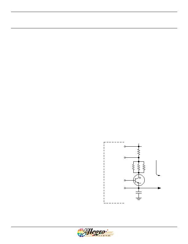
temperatures. Depending on the load requirements, using drop
resistors, as shown in figure 5, may be necessary to protect the
pass transistor from overheating.
The output current-limiting resistors, RCL (corresponding to R3
and R4), will drop between 175 mV and 225 mV at the highest
current output, I
LOAD
. Assuming no additional resistance, the
voltage dropped, V
DROP
(mV), on each pass transistor is
V
DROP
= V
REG
V
RCL
V
OUT
This can be substituted into the power dissipation formula
P
D
= V
DROP
?SPAN class="pst A8450KLBTR-T_2464169_2">
I
LOAD
Given a typical application where V
REG
= 5.8 V, V
RCL
= 0.175 V,
V
OUT
= 3.3 V, and I
LOAD
= 350 mA, then P
D
is approximately
814 mW.
Figure 5. Placement of drop resistors for thermal protection; example
shown is for the 3.3 V regulator.
VREG
CL33
V33BD
V33
V
CE
RCL
V
OUTV33
I
LOAD
A8450
V
DROP
相关PDF资料 |
PDF描述 |
|---|---|
| AMM24DSEN-S13 | CONN EDGECARD 48POS .156 EXTEND |
| EBM15MMRD | CARD MALE EXTENDER .156 30POS AU |
| W3L1YC474MAT1A | CAP CER 0.47UF 16V 20% X7R 0612 |
| H7PXH-1510G | CABLE D-SUB - HMM15H/AE15G/X |
| AMM24DSEH-S13 | CONN EDGECARD 48POS .156 EXTEND |
相关代理商/技术参数 |
参数描述 |
|---|---|
| A8450KLB-T | 功能描述:IC REG QD BUCK/LINEAR 24-SOIC RoHS:是 类别:集成电路 (IC) >> PMIC - 稳压器 - 线性 + 切换式 系列:- 标准包装:2,500 系列:- 拓扑:降压(降压)同步(2),线性(LDO)(1) 功能:任何功能 输出数:3 频率 - 开关:300kHz 电压/电流 - 输出 1:控制器 电压/电流 - 输出 2:控制器 电压/电流 - 输出 3:控制器 带 LED 驱动器:无 带监控器:无 带序列发生器:是 电源电压:4.5 V ~ 24 V 工作温度:-40°C ~ 85°C 安装类型:* 封装/外壳:28-TSSOP(0.173",4.40mm 宽) 供应商设备封装:* 包装:带卷 (TR) 其它名称:ISL6402IVZ-TTR |
| A8450KLB-T | 制造商:Allegro MicroSystems 功能描述:Voltage Regulator IC |
| A8450KLBTR | 功能描述:IC REG QD BUCK/LINEAR 24-SOIC RoHS:否 类别:集成电路 (IC) >> PMIC - 稳压器 - 线性 + 切换式 系列:- 标准包装:2,500 系列:- 拓扑:降压(降压)同步(2),线性(LDO)(1) 功能:任何功能 输出数:3 频率 - 开关:300kHz 电压/电流 - 输出 1:控制器 电压/电流 - 输出 2:控制器 电压/电流 - 输出 3:控制器 带 LED 驱动器:无 带监控器:无 带序列发生器:是 电源电压:4.5 V ~ 24 V 工作温度:-40°C ~ 85°C 安装类型:* 封装/外壳:28-TSSOP(0.173",4.40mm 宽) 供应商设备封装:* 包装:带卷 (TR) 其它名称:ISL6402IVZ-TTR |
| A8450KLBTR-T | 功能描述:IC REG QD BUCK/LINEAR 24-SOIC RoHS:是 类别:集成电路 (IC) >> PMIC - 稳压器 - 线性 + 切换式 系列:- 标准包装:2,500 系列:- 拓扑:降压(降压)同步(3),线性(LDO)(2) 功能:任何功能 输出数:5 频率 - 开关:300kHz 电压/电流 - 输出 1:控制器 电压/电流 - 输出 2:控制器 电压/电流 - 输出 3:控制器 带 LED 驱动器:无 带监控器:无 带序列发生器:是 电源电压:5.6 V ~ 24 V 工作温度:-40°C ~ 85°C 安装类型:* 封装/外壳:* 供应商设备封装:* 包装:* |
| A845DSC | 制造商:Pentair Technical Products / Hoffman 功能描述:DSC Box 8.00x4.00x4.75 Gray, 8.00x4.00x3.75, Steel |
发布紧急采购,3分钟左右您将得到回复。