- 您现在的位置:买卖IC网 > PDF目录364590 > AB-093 AB-093 - ISOLATION AMPS HIKE ACCURACY AND RELIABILITY PDF资料下载
参数资料
| 型号: | AB-093 |
| 元件分类: | 隔离放大器 |
| 英文描述: | AB-093 - ISOLATION AMPS HIKE ACCURACY AND RELIABILITY |
| 中文描述: | 抗体- 093 -分离AMPS二元调涨精确度和可靠性 |
| 文件页数: | 1/2页 |
| 文件大小: | 22K |
| 代理商: | AB-093 |
90
A
APPLICATION BULLE TIN
Mailing Address: PO Box 11400 Tucson, AZ 85734 Street Address: 6730 S. Tucson Blvd. Tucson, AZ 85706
Tel: (602) 746-1111 Twx: 910-952-111 Telex: 066-6491 FAX (602) 889-1510 Immediate Product Info: (800) 548-6132
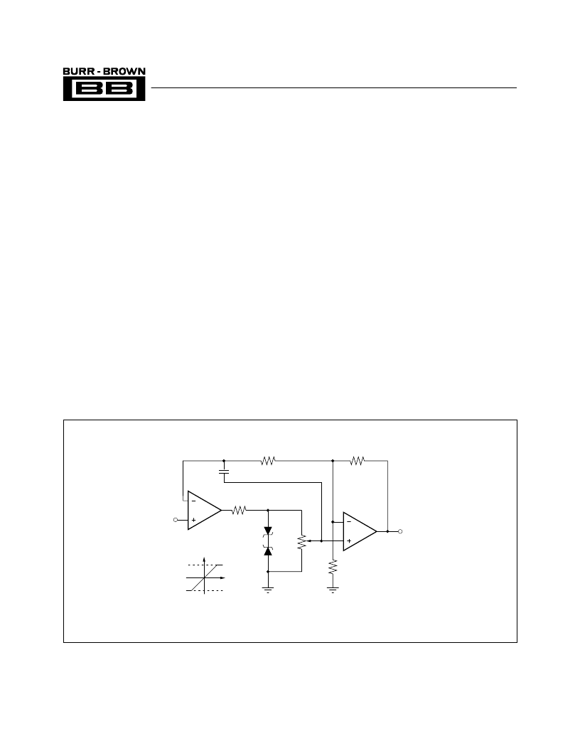
A limiter circuit consisting of an input buffer (A
), an
output-scaling amplifier (A
), two zener diodes (Z
and Z
),
and several other components can supply sharp, precise,
bipolar clamp levels with continuous variable control, from
0 to
±
11V. See Figure 1. A feedback loop enclosing the
amplifiers and zeners generates the high clamping accuracy.
Within the limit range of the clamp (
±
V
), the zener diodes
are off, and A
2
feeds back its output to the inverting input of
A
through R
. At the same time A
drives A
through the
voltage divider R
. The feedback forces the inverting input
of op amp A
1
to equal E
I
at the noninverting input terminal.
The circuit forces the inverting input of A
2
also to follow E
I
.
There’s no signal voltage drop across R
, because no current
can flow from it into A
2
’s inverting input. Consequently, the
noninverting input of A
2
, which defines the potentiometer
output at feedback equilibrium, must also track E
. A resistor
voltage divider can replace the control potentiometer R
V
in
fixed-level limiting applications.
Amplifier A
2
then delivers an output:
E
O
= (1 + R
3
/R
2
) E
I
when
–V
L
< E
O
< V
L
and
V
L
= x [(1 + R
3
/R
2
)] (V
Z
+ V
F
)
where x is the setting fraction of R
, and V
and V
are the
zener and forward voltages, respectively. The overall circuit
response, then, is simply that of a voltage amplifier when the
output signal is within the limit boundaries.
Amplifier A
generates small deviations from an ideal re-
sponse because A
’s circuit gain (1 + R
/R
) amplifies any
offset voltage and noise from A
1
. Similarly, this loop gain
mitigates the clamping error by sharpening its clamping
response. The zener drive increases during the transition to
the clamping state.
FIGURE 1. Amplifier A
Buffers and Amplifier A
Scales Input Signals Under Feedback Control. Zener diodes and a
potentiometer or voltage divider in the feedback loop supply a continuously variable bipolar-clamping limit.
FEEDBACK CIRCUIT CLAMPS PRECISELY
by Jerald Graeme, (602) 746-7412
A
2
A
1
1k
R
1
E
I
1k
R
4
10k
R
3
E
O
C
2200pF
1N4626
Z
1
Z
2
R
2
13k
1/2
OPA2111
R
V
20k
1/2
OPA2111
E
O
E
I
–V
L
V
L
E
= (1 + R
3
/R
) E
I
,
for –V
L
< E
O
< V
V
L
= x(1 + R
3
/R
2
)(V
Z
+ V
F
)
1994 Burr-Brown Corporation
AB-090
Printed in U.S.A. January, 1994
相关PDF资料 |
PDF描述 |
|---|---|
| AB-094 | AB-094 - TAME PHOTODIODES WITH OP AMP BOOTSTRAP |
| AB-095 | AB-095 - TIPS FOR USING THE ADS78XX FAMILY OF A/D CONVERTERS |
| AB-096 | AB-096 - BUILD A THREE PHASE SINE WAVE GENERATOR WITH THE UAF42 |
| AB-097 | AB-097 - DDC101 EVALUATION FIXTURE PC INTERFACE BOARD |
| AB-098 | AB-098 - SELECTING AN A/D CONVERTER |
相关代理商/技术参数 |
参数描述 |
|---|---|
| AB-094 | 制造商:未知厂家 制造商全称:未知厂家 功能描述:AB-094 - TAME PHOTODIODES WITH OP AMP BOOTSTRAP |
| AB-095 | 制造商:未知厂家 制造商全称:未知厂家 功能描述:AB-095 - TIPS FOR USING THE ADS78XX FAMILY OF A/D CONVERTERS |
| AB-096 | 制造商:未知厂家 制造商全称:未知厂家 功能描述:AB-096 - BUILD A THREE PHASE SINE WAVE GENERATOR WITH THE UAF42 |
| AB-097 | 制造商:未知厂家 制造商全称:未知厂家 功能描述:AB-097 - DDC101 EVALUATION FIXTURE PC INTERFACE BOARD |
| AB-098 | 制造商:未知厂家 制造商全称:未知厂家 功能描述:AB-098 - SELECTING AN A/D CONVERTER |
发布紧急采购,3分钟左右您将得到回复。