参数资料
| 型号: | ACS8944T |
| 厂商: | Semtech |
| 文件页数: | 20/24页 |
| 文件大小: | 0K |
| 描述: | IC JITTER ATT MULT PLL 48-QFN |
| 标准包装: | 1 |
| 类型: | 时钟/频率发生器,多路复用器 |
| PLL: | 是 |
| 主要目的: | SONET/SDH |
| 输入: | LVPECL |
| 输出: | LVPECL |
| 电路数: | 1 |
| 比率 - 输入:输出: | 1:1 |
| 差分 - 输入:输出: | 是/是 |
| 频率 - 最大: | 155.52MHz |
| 电源电压: | 3.135 V ~ 3.465 V |
| 工作温度: | -40°C ~ 85°C |
| 安装类型: | 表面贴装 |
| 封装/外壳: | 48-VFQFN 裸露焊盘 |
| 供应商设备封装: | 48-QFN(7x7) |
| 包装: | 管件 |
ADVANCED COMMUNICATIONS
FINAL
DATASHEET
Revision 3/November 2006 Semtech Corp.
Page 5
www.semtech.com
ACS8944 JAM PLL
Note...I = Input, O = Output, P = Power, LVTTL/LVCMOSU = LVTTL/LVCMOS input with pull-up resistor, LVTTL/LVCMOSD = LVTTL/LVCMOS input
with pull-down resistor
The ACS8944 is a low jitter integrated PLL for clock
dejittering and clock rate translation, meeting the jitter
requirements for SONET up to and including OC-12
(622.08 MHz systems). It is compliant to the relevant ITU,
Telcordia/Bellcore and ETSI standards for at least OC-3
(155.52 MHz) and OC-12 (622.08 MHz) - equivalent to
the corresponding STM-1 and STM-4 rates.
It can be configured for a range of applications using a
minimal number of external components and is available
in a small form factor QFN48 package at 7 mm x 7 mm x
0.9 mm outer dimensions.
Input
The ACS8944 has a single, LVPECL, differential input
(CLKN/P, pins 27 and 28). It is designed to operate with
any of 19.44 MHz, 38.88 MHz, 77.76 MHz or
155.52 MHz input references, and can pull in an input
which is within ±400 ppm of these spot frequencies.
Input Configuration
The input must be configured for the expected input
frequency. This is achieved by connecting the EXT[3:1]
pins, to the configuration pins or to power (VDD) or ground
(VSS), in accordance with the configuration scheme in
Table 4, e.g. for an expected input of 155.52 MHz,
connect EXT1 to VSS, EXT2 to CFG_OUT1 and EXT3 to
CFG_OUT3.
Output
The ACS8944 has a single, LVPECL, differential output
(OUTN/P, pins 2 and 3).
The frequency of the output is determined by the wiring of
OP_FSEL to the appropriate CFG_OUT pin in accordance
with Table 5.
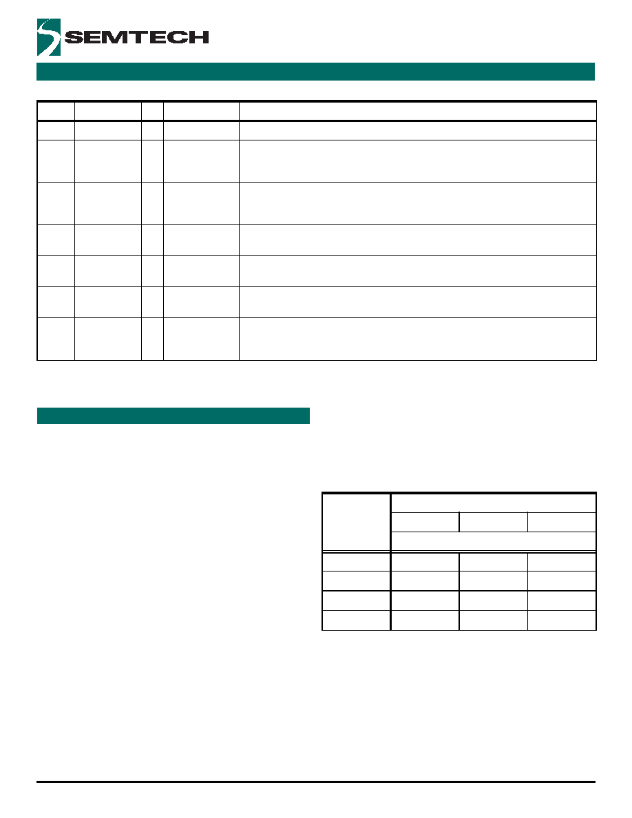
24
EXT3
I
27
CLKN
I
LVPECL
Input reference clock to which the PLL will phase and frequency lock (negative pin of
differential pair, partnered with pin 28). Can accept 19.44 MHz, 38.88 MHz, 77.76 MHz or
155.52 MHz to within ±400 ppm.
28
CLKP
I
LVPECL
Input reference clock to which the PLL will phase and frequency lock (positive pin of
differential pair, partnered with pin 27). Can accept 19.44 MHz, 38.88 MHz, 77.76 MHz or
155.52 MHz to within ±400 ppm.
35
VCP
I/O
Analog
Connection for external loop filter components. This is the differential control voltage input
to the internal VCO and the internal differential charge pump output.
36
VCN
I/O
Analog
Connection for external loop filter components. This is the differential control voltage input
to the internal VCO and the internal differential charge pump output.
40
RESETB
I
LVTTL/LVCMOSU
Schmitt Trigger
Active low reset signal with pull up and Schmitt type input. Used to apply a Power On Reset
(POR) signal during system initialization. Should be connected via a capacitor to ground.
46
OP_FSEL
I
LVTTL/
LVCMOSD
Output Frequency Select Pin. Used with the Output Frequency Configuration pins (pins 13
to 16) to configure the output frequency (on power-up/reset) of the differential output
OUT(N/P). See Table 5.
Table 3 Functional Pins (cont...)
Pin No.
Symbol
I/O
Type
Description
Table 4 Input Frequency Selection
For Expected
Input
Frequency
of
Connect
EXT1
EXT2
EXT3
to
19.44 MHz
CFG_OUT3
VDD
CFG_OUT3
38.88 MHZ
CFG_OUT0
CFG_OUT1
CFG_OUT3
77.76 MHz
VDD
CFG_OUT3
155.52 MHz
VSS
CFG_OUT1
CFG_OUT3
相关PDF资料 |
PDF描述 |
|---|---|
| ACS8946T | IC JITTER ATT MULT PLL 48-QFN |
| ACS8947T | IC JITTER ATT MULT PLL 48-QFN |
| AD10200BZ | IC ADC DUAL 12BIT 68-CLCC |
| AD10242BZ | IC ADC DUAL 12BIT 68-CLCC |
| AD10465BZ | IC ADC DUAL 14BIT 68-CLCC |
相关代理商/技术参数 |
参数描述 |
|---|---|
| ACS8946 | 制造商:SEMTECH 制造商全称:Semtech Corporation 功能描述:Jitter Attenuating, Multiplying Phase Locked Loop, with Protection Switch, for OC-12/STM-4 and GbE |
| ACS8946EVB | 制造商:SEMTECH 制造商全称:Semtech Corporation 功能描述:Jitter Attenuating, Multiplying Phase Locked Loop, with Protection Switch, for OC-12/STM-4 and GbE |
| ACS8946T | 功能描述:IC JITTER ATT MULT PLL 48-QFN RoHS:是 类别:集成电路 (IC) >> 时钟/计时 - 专用 系列:- 标准包装:1,500 系列:- 类型:时钟缓冲器/驱动器 PLL:是 主要目的:- 输入:- 输出:- 电路数:- 比率 - 输入:输出:- 差分 - 输入:输出:- 频率 - 最大:- 电源电压:3.3V 工作温度:0°C ~ 70°C 安装类型:表面贴装 封装/外壳:28-SSOP(0.209",5.30mm 宽) 供应商设备封装:28-SSOP 包装:带卷 (TR) 其它名称:93786AFT |
| ACS8947T | 功能描述:IC JITTER ATT MULT PLL 48-QFN RoHS:是 类别:集成电路 (IC) >> 时钟/计时 - 专用 系列:- 标准包装:1,500 系列:- 类型:时钟缓冲器/驱动器 PLL:是 主要目的:- 输入:- 输出:- 电路数:- 比率 - 输入:输出:- 差分 - 输入:输出:- 频率 - 最大:- 电源电压:3.3V 工作温度:0°C ~ 70°C 安装类型:表面贴装 封装/外壳:28-SSOP(0.209",5.30mm 宽) 供应商设备封装:28-SSOP 包装:带卷 (TR) 其它名称:93786AFT |
| ACS9010 | 制造商:未知厂家 制造商全称:未知厂家 功能描述:Optoelectronic |
发布紧急采购,3分钟左右您将得到回复。