参数资料
| 型号: | AD1893JSTZ |
| 厂商: | Analog Devices Inc |
| 文件页数: | 3/20页 |
| 文件大小: | 0K |
| 描述: | IC SAMPLE-RATE CONV 16BIT 44TQFP |
| 标准包装: | 1 |
| 系列: | SamplePort™ |
| 类型: | 采样率转换器 |
| 应用: | 多媒体 |
| 安装类型: | 表面贴装 |
| 封装/外壳: | 44-LQFP |
| 供应商设备封装: | 44-LQFP(10x10) |
| 包装: | 托盘 |
AD1893
REV. A
–11–
Sample Clock Jitter Rejection
The loop filter settling time also affects the ability of the
AD1893 ASRC to reject sample clock jitter, since the control
loop effectively computes a time weighted average or “esti-
mated” new output of many past input and output clock events.
This first order low pass filtering of the sample clock ratio pro-
vides the AD1893 with its jitter rejection characteristic. In the
slow settling mode, the AD1893 attenuates jitter frequencies
higher than 3 Hz (
≈800 ms for the control loop to settle to an
18-bit “pure” sine wave), and thus rejects all but the most se-
vere sample clock jitter; performance is essentially limited only
by the FIR filter. In the fast settling mode, the ASRC attenuates
jitter components above 12 Hz (
≈200 ms for the control loop to
settle). Due to the effects of on-chip synchronization of the
sample clocks to the 16 MHz (62.5 ns) crystal master clock,
sample clock jitter must be a large percentage of the crystal
period (>10 ns) before performance degrades in either the slow
or fast settling modes. Note that since both past input and past
output clocks are used to compute the filtered “current” internal
output clock request, jitter on both the input sample clock and
the output sample clock is rejected equally. In summary: the fast-
settling mode is best for applications when the sample rates will
be dynamically altered (e.g., varispeed situations), while the
slow-settling mode provides the most sample clock jitter rejection.
Clock jitter can be modeled as a frequency modulation process.
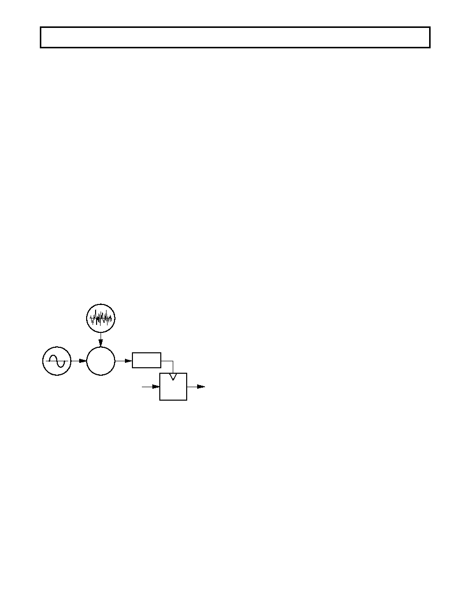
Figure 7 shows one such model, where a noise source combined
with a sine wave source modulates the “carrier” frequency gen-
erated by a voltage controlled oscillator.
NOISE SOURCE
VCO
DIGITAL
OUT
ANALOG IN
ADC
VOLTAGE
SOURCE
Σ
NOISE
WAVEFORM
SINE
WAVE
Figure 7. Clock Jitter Modeled as a Modulated VCO
If the jittered output of the VCO is used to clock an analog-to-
digital converter, the digital output of the ADC will be contami-
nated by the presence of jitter. If the noise source is spectrally
flat (i.e., “white” jitter), an FFT of the ADC digital output
would show a spectrum with a uniform noise floor that is
elevated compared to the spectrum with the noise source turned
off. If the noise source has distinct frequency components (i.e.,
“correlated” jitter), then an FFT of the ADC digital output
would show symmetrical sidebands around the ADC input
signal, at amplitudes and frequencies determined by frequency
modulation theory. One notable result is that the level of the
noise or the sidebands is proportional to the slope of the input
signal, i.e., the worst case occurs at the highest frequency full-
scale input (a full-scale 20 kHz sinusoid).
The AD1893 applies rejection to these jitter frequency compo-
nents referenced to the input signal. In other words, if a 5 kHz
digital sinusoid is applied to the ASRC, depending on the set-
tling mode selected, the ASRC will attenuate sample clock jitter
at either 3 Hz above and below 5 kHz (slow settling) or 12 Hz
above and below 5 kHz (fast settling). The rolloff is 6 dB per
octave. As an example, suppose there was correlated jitter
present on the input sample clock with a 1 kHz component,
associated with the same 5 kHz sinusoidal input data. This
would produce sidebands at 4 kHz and 6 kHz, 3 kHz and
7 kHz, etc., with amplitudes that decrease as they move away
from the input signal frequency. For the slow-settling mode
case, 1 kHz represents more than nine octaves (relative to
3 Hz), so the first two sideband pairs would be attenuated by
more than 54 dB. For the fast-settling mode case, 1 kHz repre-
sents more than seven octaves (relative to 12 Hz), so that the
first two sideband pairs would be attenuated by more than 42 dB.
The second and higher sideband pairs are attenuated even more
because they are spaced further from the input signal frequency.
Group Delay Modes
The other parameter that determines the likelihood of FIFO
input overflow or output underflow is the FIFO depth. This
FIFO induced group delay is better termed transport delay,
since it is frequency independent, and should be kept conceptu-
ally distinct from the notion of group delay as used in the poly-
phase filter bank model. The total group delay of the AD1893
equals the FIFO transport delay plus the FIR (polyphase) filter
group delay.
In the AD1893, the FIFO read and write pointers are separated
by five memory locations (
≈100 s equivalent transport delay at
a 50 kHz sample rate). This is added to the FIR filter delay
(64 taps divided by 2) for a total nominal group delay in short
mode of
≈700 s.
This delay is deterministic and constant except when FSOUT
drops below FSIN which causes the number of FIR filter taps to
increase (see Cutoff Frequency Modification section). If the
FIFO read and write addresses cross, the MUTE_O signal will
be asserted. Note that under all conditions, both the highly
oversampled low-pass prototype and the polyphase subfilters of
the AD1893 ASRC possess a linear phase response.
相关PDF资料 |
PDF描述 |
|---|---|
| AD1895AYRSZRL | IC SAMP-RATEHP/CONV 24BIT 28SSOP |
| AD1896AYRSZRL | IC SAMP-RATEHP/CONV 24BIT 28SSOP |
| AD1940YSTZ | IC DSP AUDIO 16CH/28BIT 48-LQFP |
| AD246JY | IC CLK BUFF DVR 1:1 25KHZ 13-SIP |
| AD532SD | IC MULTIPLIER +/-10V 14-CDIP |
相关代理商/技术参数 |
参数描述 |
|---|---|
| AD1893JSTZRL | 功能描述:IC SAMPLE-RATE CONV 16BIT 44TQFP RoHS:是 类别:集成电路 (IC) >> 线性 - 音频处理 系列:SamplePort™ 其它有关文件:STA321 View All Specifications 标准包装:1 系列:Sound Terminal™ 类型:音频处理器 应用:数字音频 安装类型:表面贴装 封装/外壳:64-LQFP 裸露焊盘 供应商设备封装:64-LQFP EP(10x10) 包装:Digi-Reel® 其它名称:497-11050-6 |
| AD1895 | 制造商:AD 制造商全称:Analog Devices 功能描述:192 kHz Stereo Asynchronous Sample Rate Converter |
| AD1895AYRS | 制造商:Analog Devices 功能描述:Sample Rate Converter 28-Pin SSOP 制造商:Rochester Electronics LLC 功能描述:192KHZ 8:1 STEREO ASYNC SAMPLE RATE CONV - Bulk 制造商:Analog Devices 功能描述:IC STEREO ASR CONVERTER |
| AD1895AYRSRL | 制造商:Analog Devices 功能描述:Sample Rate Converter 28-Pin SSOP T/R |
| AD1895AYRSZ | 功能描述:IC CONV SAMPLE RATE ASYNC 28SSOP RoHS:是 类别:集成电路 (IC) >> 线性 - 音频处理 系列:- 其它有关文件:STA321 View All Specifications 标准包装:1 系列:Sound Terminal™ 类型:音频处理器 应用:数字音频 安装类型:表面贴装 封装/外壳:64-LQFP 裸露焊盘 供应商设备封装:64-LQFP EP(10x10) 包装:Digi-Reel® 其它名称:497-11050-6 |
发布紧急采购,3分钟左右您将得到回复。