- 您现在的位置:买卖IC网 > PDF目录10950 > AD1939WBSTZ (Analog Devices Inc)AUDIO CODEC W/ON CHIP 4ADC 8DAC PDF资料下载
参数资料
| 型号: | AD1939WBSTZ |
| 厂商: | Analog Devices Inc |
| 文件页数: | 6/32页 |
| 文件大小: | 0K |
| 描述: | AUDIO CODEC W/ON CHIP 4ADC 8DAC |
| 标准包装: | 1 |
| 类型: | 通用 |
| 数据接口: | 串行 |
| 分辨率(位): | 24 b |
| ADC / DAC 数量: | 4 / 8 |
| 三角积分调变: | 是 |
| S/N 比,标准 ADC / DAC (db): | 94 / 94 |
| 动态范围,标准 ADC / DAC (db): | 105 / 110 |
| 电压 - 电源,模拟: | 3 V ~ 3.6 V |
| 电压 - 电源,数字: | 3 V ~ 3.6 V |
| 工作温度: | -40°C ~ 105°C |
| 安装类型: | 表面贴装 |
| 封装/外壳: | 64-LQFP |
| 供应商设备封装: | 64-LQFP(10x10) |
| 包装: | 托盘 |
第1页第2页第3页第4页第5页当前第6页第7页第8页第9页第10页第11页第12页第13页第14页第15页第16页第17页第18页第19页第20页第21页第22页第23页第24页第25页第26页第27页第28页第29页第30页第31页第32页
AD1939
Data Sheet
Rev. E | Page 14 of 32
master clock. In addition, it is especially important that the
clock signal not pass through an FPGA, CPLD, or other large
digital chip (such as a DSP) before being applied to the
AD1939. In most cases, this induces clock jitter due to the
sharing of common power and ground connections with other
unrelated digital output signals. When the PLL is used, jitter in
the reference clock is attenuated above a certain frequency
depending on the loop filter.
RESET AND POWER-DOWN
The function of the RST pin sets all the control registers to their
default settings. To avoid pops, reset does not power down the
analog outputs. After RST is deasserted and the PLL acquires
lock condition, an initialization routine runs inside the
AD1939. This initialization lasts for approximately 256 master
clock cycles.
The power-down bits in the PLL and Clock Control 0, DAC
Control 1, and ADC Control 1 registers power down the
respective sections. All other register settings are retained. To
guarantee proper startup, the RST pin should be pulled low by
an external resistor.
SERIAL CONTROL PORT
The AD1939 has an SPI control port that permits programming
and reading back of the internal control registers for the ADCs,
DACs, and clock system. A standalone mode is also available
for operation without serial control; standalone is configured at
reset by connecting CIN, CCLK, and CLATCH to ground. In
standalone mode, all registers are set to default, except the
internal MCLK enable, which is set to 1. The ADC, ABCLK, and
ALRCLK clock ports are set to master/slave by the connecting
the COUT pin to either DVDD or ground. Standalone mode
only supports stereo mode with an I2S data format and 256 fS
MCLK rate. Refer to Table 11 for details. If CIN, CCLK, and
CLATCH are not grounded, the AD1939 SPI port is active. It is
recommended to use a weak pull-up resistor on CLATCHin
applications that have a microcontroller. This pull-up resistor
ensures that the AD1939 recognizes the presence of a
microcontroller.
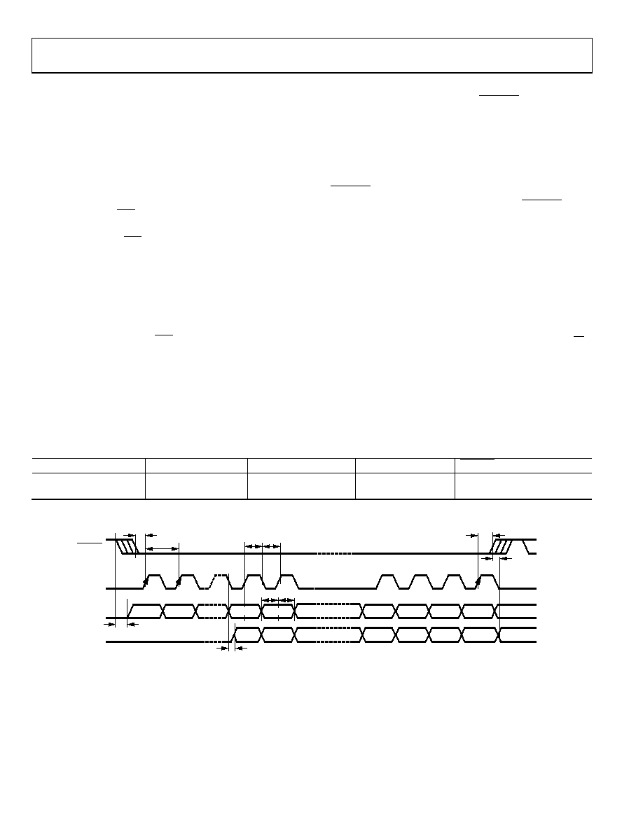
The SPI control port of the AD1939 is a 4-wire serial control
port. The format is similar to the Motorola SPI format except
the input data-word is 24 bits wide. The serial bit clock and
latch can be completely asynchronous to the sample rate of the
ADCs and DACs. Figure 11 shows the format of the SPI signal.
The first byte is a global address with a read/write bit. For the
AD1939, the address is 0x04, shifted left one bit due to the R/W
bit. The second byte is the AD1939 register address and the
third byte is the data.
Table 11. Standalone Mode Selection
ADC Clocks
CIN
COUT
CCLK
CLATCH
Slave
0
Master
0
1
0
D0
D8
D22
D23
D9
CLATCH
CCLK
CIN
COUT
tCCH tCCL
tCDS tCDH
tCLS
tCCP
tCLH
tCOTS
tCOD
tCOE
06
07
1-
0
10
Figure 11. Format of the SPI Signal
相关PDF资料 |
PDF描述 |
|---|---|
| MCF5253VM140J | IC MCU 2.1MIPS 140MHZ 225MAPBGA |
| MCF5253VM140 | IC MCU 32BIT 225-MAPBGA |
| ADAV801ASTZ | IC CODEC AUDIO R-DVD 3.3V 64LQFP |
| MCIMX27LVOP4AR2 | IC LOW END I.MX27 404-MAPBGA |
| AD1938YSTZ | IC CODEC 24BIT 4ADC/8DAC 48LQFP |
相关代理商/技术参数 |
参数描述 |
|---|---|
| AD1939WBSTZ-RL | 功能描述:AUDIO CODEC W/ON CHIP 4ADC 8DAC RoHS:是 类别:集成电路 (IC) >> 接口 - 编解码器 系列:- 标准包装:2,500 系列:- 类型:立体声音频 数据接口:串行 分辨率(位):18 b ADC / DAC 数量:2 / 2 三角积分调变:是 S/N 比,标准 ADC / DAC (db):81.5 / 88 动态范围,标准 ADC / DAC (db):82 / 87.5 电压 - 电源,模拟:2.6 V ~ 3.3 V 电压 - 电源,数字:1.7 V ~ 3.3 V 工作温度:-40°C ~ 85°C 安装类型:表面贴装 封装/外壳:48-WFQFN 裸露焊盘 供应商设备封装:48-TQFN-EP(7x7) 包装:带卷 (TR) |
| AD1939XSTZ | 制造商:Analog Devices 功能描述:AUD CODEC 4ADC / 8DAC 24BIT 64LQFP - Trays |
| AD1939XSTZRL | 制造商:AD 制造商全称:Analog Devices 功能描述:4 ADC/8 DAC with PLL, 192 kHz, 24 Bit CODEC |
| AD1939YSTZ | 功能描述:IC CODEC 24BIT ADC/DAC 64LQFP RoHS:是 类别:集成电路 (IC) >> 接口 - 编解码器 系列:- 标准包装:2,500 系列:- 类型:PCM 数据接口:PCM 音频接口 分辨率(位):15 b ADC / DAC 数量:1 / 1 三角积分调变:是 S/N 比,标准 ADC / DAC (db):- 动态范围,标准 ADC / DAC (db):- 电压 - 电源,模拟:2.7 V ~ 3.3 V 电压 - 电源,数字:2.7 V ~ 3.3 V 工作温度:-40°C ~ 85°C 安装类型:表面贴装 封装/外壳:80-VFBGA 供应商设备封装:80-BGA MICROSTAR JUNIOR(5x5) 包装:带卷 (TR) 其它名称:296-21257-2 |
| AD1939YSTZRL | 功能描述:IC CODEC 24BIT ADC/DAC 64-LQFP RoHS:是 类别:集成电路 (IC) >> 接口 - 编解码器 系列:- 标准包装:2,500 系列:- 类型:立体声音频 数据接口:串行 分辨率(位):18 b ADC / DAC 数量:2 / 2 三角积分调变:是 S/N 比,标准 ADC / DAC (db):81.5 / 88 动态范围,标准 ADC / DAC (db):82 / 87.5 电压 - 电源,模拟:2.6 V ~ 3.3 V 电压 - 电源,数字:1.7 V ~ 3.3 V 工作温度:-40°C ~ 85°C 安装类型:表面贴装 封装/外壳:48-WFQFN 裸露焊盘 供应商设备封装:48-TQFN-EP(7x7) 包装:带卷 (TR) |
发布紧急采购,3分钟左右您将得到回复。