- 您现在的位置:买卖IC网 > PDF目录10950 > AD1939WBSTZ (Analog Devices Inc)AUDIO CODEC W/ON CHIP 4ADC 8DAC PDF资料下载
参数资料
| 型号: | AD1939WBSTZ |
| 厂商: | Analog Devices Inc |
| 文件页数: | 7/32页 |
| 文件大小: | 0K |
| 描述: | AUDIO CODEC W/ON CHIP 4ADC 8DAC |
| 标准包装: | 1 |
| 类型: | 通用 |
| 数据接口: | 串行 |
| 分辨率(位): | 24 b |
| ADC / DAC 数量: | 4 / 8 |
| 三角积分调变: | 是 |
| S/N 比,标准 ADC / DAC (db): | 94 / 94 |
| 动态范围,标准 ADC / DAC (db): | 105 / 110 |
| 电压 - 电源,模拟: | 3 V ~ 3.6 V |
| 电压 - 电源,数字: | 3 V ~ 3.6 V |
| 工作温度: | -40°C ~ 105°C |
| 安装类型: | 表面贴装 |
| 封装/外壳: | 64-LQFP |
| 供应商设备封装: | 64-LQFP(10x10) |
| 包装: | 托盘 |
第1页第2页第3页第4页第5页第6页当前第7页第8页第9页第10页第11页第12页第13页第14页第15页第16页第17页第18页第19页第20页第21页第22页第23页第24页第25页第26页第27页第28页第29页第30页第31页第32页
Data Sheet
AD1939
Rev. E | Page 15 of 32
POWER SUPPLY AND VOLTAGE REFERENCE
The AD1939 is designed for 3.3 V supplies. Separate power
supply pins are provided for the analog and digital sections.
To minimize noise pickup, these pins should be bypassed with
100 nF ceramic chip capacitors placed as close to the pins as
possible. A bulk aluminum electrolytic capacitor of at least
22 μF should also be provided on the same PC board as the
codec. For critical applications, improved performance is
obtained with separate supplies for the analog and digital sections.
If this is not possible, it is recommended that the analog and
digital supplies be isolated by means of a ferrite bead in series
with each supply. It is important that the analog supply be as
clean as possible.
The AD1939 includes a 3.3 V regulator driver that only requires
an external pass transistor and bypass capacitors to make a 5 V
to 3.3 V regulator. If the regulator driver is not used, connect
VSUPPLY, VDRIVE, and VSENSE to DGND.
All digital inputs are compatible with TTL and CMOS levels.
All outputs are driven from the 3.3 V DVDD supply and are
compatible with TTL and 3.3 V CMOS levels.
The ADC and DAC internal voltage reference (VREF) is brought
out on FILTR and should be bypassed as close as possible to the
chip with a parallel combination of 10 μF and 100 nF. Any
external current drawn should be limited to less than 50 μA.
The internal reference can be disabled in the PLL and Clock
Control 1 register and FILTR can be driven from an external
source. This can be used to scale the DAC output to the clipping
level of a power amplifier based on its power supply voltage.
The ADC input gain varies by the inverse ratio. The total gain
from ADC input to DAC output remains constant.
The CM pin is the internal common-mode reference. It should
be bypassed as close as possible to the chip, with a parallel
combination of 47 μF and 100 nF. This voltage can be used to
bias external op amps to the common-mode voltage of the input
and output signal pins. The output current should be limited to
less than 0.5 mA source and 2 mA sink.
SERIAL DATA PORTS—DATA FORMAT
The eight DAC channels use a common serial bit clock (DBCLK)
and a common left-right framing clock (DLRCLK) in the serial
data port. The four ADC channels use a common serial bit
clock (ABCLK) and left-right framing clock (ALRCLK) in the
serial data port. The clock signals are all synchronous with the
sample rate. The normal stereo serial modes are shown in
The ADC and DAC serial data modes default to I2S. The ports
can also be programmed for left-justified, right-justified, and
TDM modes. The word width is 24 bits by default and can be
programmed for 16 or 20 bits. The DAC serial formats are
programmable according to the DAC Control 0 register. The
polarity of DBCLK and DLRCLK is programmable according to
the DAC Control 1 register. The ADC serial formats and serial
clock polarity are programmable according to the ADC Control 1
register. Both DAC and ADC serial ports are programmable to
become the bus masters according to DAC Control 1 register
and ADC Control 2 register. By default, both ADC and DAC
serial ports are in the slave mode.
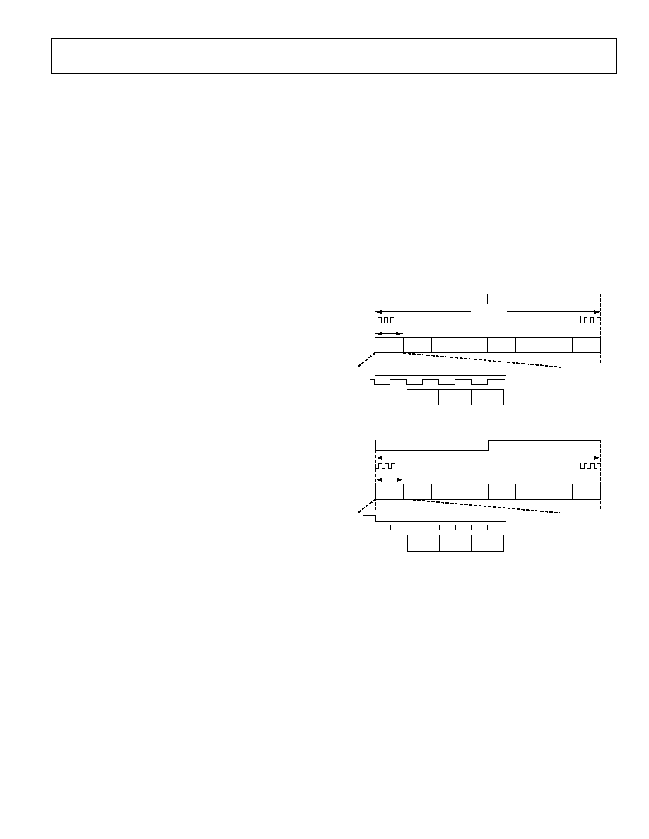
TIME-DIVISION MULTIPLEXED (TDM) MODES
The AD1939 serial ports also have several different TDM serial
data modes. The first and most commonly used configurations
serial port outputs one data stream consisting of four on-chip
ADCs followed by four unused slots. In Figure 13, the eight on-
chip DAC data slots are packed into one TDM stream. In this
mode, both DBCLK and ABCLK are 256 fS.
SLOT 1
LEFT 1
SLOT 2
RIGHT 1
SLOT 3
LEFT 2
SLOT 4
RIGHT 2
MSB
MSB–1
MSB–2
DATA
BCLK
LRCLK
SLOT 5
SLOT 6
SLOT 7
SLOT 8
LRCLK
BCLK
DATA
256 BCLKs
32 BCLKs
0
6
07
1-
0
16
Figure 12. ADC TDM (8-Channel I2S Mode)
SLOT 1
LEFT 1
SLOT 2
RIGHT 1
SLOT 3
LEFT 2
SLOT 4
RIGHT 2
MSB
MSB–1
MSB–2
DATA
BCLK
LRCLK
SLOT 5
LEFT 3
SLOT 6
RIGHT 3
SLOT 7
LEFT 4
SLOT 8
RIGHT 4
LRCLK
BCLK
DATA
256 BCLKs
32 BCLKs
0
60
71-
01
7
Figure 13. DAC TDM (8-Channel I2S Mode)
The I/O pins of the serial ports are defined according to the
serial mode that is selected. For a detailed description of the
function of each pin in TDM and AUX modes, see Table 12.
The AD1939 allows systems with more than eight DAC channels
to be easily configured by the use of an auxiliary serial data port.
The DAC TDM-AUX mode is shown in Figure 14. In this mode,
the AUX channels are the last four slots of the TDM data stream.
These slots are extracted and output to the AUX serial port. It
should be noted that due to the high DBCLK frequency, this mode
is available only in the 48 kHz/44.1 kHz/32 kHz sample rate.
The AD1939 also allows system configurations with more than
four ADC channels as shown in Figure 15 (using 8 ADCs) and
Figure 16 (using 16 ADCs). Again, due to the high ABCLK fre-
quency, this mode is available only in the 48 kHz/44.1 kHz/32 kHz
sample rate.
相关PDF资料 |
PDF描述 |
|---|---|
| MCF5253VM140J | IC MCU 2.1MIPS 140MHZ 225MAPBGA |
| MCF5253VM140 | IC MCU 32BIT 225-MAPBGA |
| ADAV801ASTZ | IC CODEC AUDIO R-DVD 3.3V 64LQFP |
| MCIMX27LVOP4AR2 | IC LOW END I.MX27 404-MAPBGA |
| AD1938YSTZ | IC CODEC 24BIT 4ADC/8DAC 48LQFP |
相关代理商/技术参数 |
参数描述 |
|---|---|
| AD1939WBSTZ-RL | 功能描述:AUDIO CODEC W/ON CHIP 4ADC 8DAC RoHS:是 类别:集成电路 (IC) >> 接口 - 编解码器 系列:- 标准包装:2,500 系列:- 类型:立体声音频 数据接口:串行 分辨率(位):18 b ADC / DAC 数量:2 / 2 三角积分调变:是 S/N 比,标准 ADC / DAC (db):81.5 / 88 动态范围,标准 ADC / DAC (db):82 / 87.5 电压 - 电源,模拟:2.6 V ~ 3.3 V 电压 - 电源,数字:1.7 V ~ 3.3 V 工作温度:-40°C ~ 85°C 安装类型:表面贴装 封装/外壳:48-WFQFN 裸露焊盘 供应商设备封装:48-TQFN-EP(7x7) 包装:带卷 (TR) |
| AD1939XSTZ | 制造商:Analog Devices 功能描述:AUD CODEC 4ADC / 8DAC 24BIT 64LQFP - Trays |
| AD1939XSTZRL | 制造商:AD 制造商全称:Analog Devices 功能描述:4 ADC/8 DAC with PLL, 192 kHz, 24 Bit CODEC |
| AD1939YSTZ | 功能描述:IC CODEC 24BIT ADC/DAC 64LQFP RoHS:是 类别:集成电路 (IC) >> 接口 - 编解码器 系列:- 标准包装:2,500 系列:- 类型:PCM 数据接口:PCM 音频接口 分辨率(位):15 b ADC / DAC 数量:1 / 1 三角积分调变:是 S/N 比,标准 ADC / DAC (db):- 动态范围,标准 ADC / DAC (db):- 电压 - 电源,模拟:2.7 V ~ 3.3 V 电压 - 电源,数字:2.7 V ~ 3.3 V 工作温度:-40°C ~ 85°C 安装类型:表面贴装 封装/外壳:80-VFBGA 供应商设备封装:80-BGA MICROSTAR JUNIOR(5x5) 包装:带卷 (TR) 其它名称:296-21257-2 |
| AD1939YSTZRL | 功能描述:IC CODEC 24BIT ADC/DAC 64-LQFP RoHS:是 类别:集成电路 (IC) >> 接口 - 编解码器 系列:- 标准包装:2,500 系列:- 类型:立体声音频 数据接口:串行 分辨率(位):18 b ADC / DAC 数量:2 / 2 三角积分调变:是 S/N 比,标准 ADC / DAC (db):81.5 / 88 动态范围,标准 ADC / DAC (db):82 / 87.5 电压 - 电源,模拟:2.6 V ~ 3.3 V 电压 - 电源,数字:1.7 V ~ 3.3 V 工作温度:-40°C ~ 85°C 安装类型:表面贴装 封装/外壳:48-WFQFN 裸露焊盘 供应商设备封装:48-TQFN-EP(7x7) 包装:带卷 (TR) |
发布紧急采购,3分钟左右您将得到回复。