- 您现在的位置:买卖IC网 > PDF目录10965 > AD1970JSTZRL (Analog Devices Inc)IC ENCODER BTSC W/CODEC 48-LQFP PDF资料下载
参数资料
| 型号: | AD1970JSTZRL |
| 厂商: | Analog Devices Inc |
| 文件页数: | 18/20页 |
| 文件大小: | 0K |
| 描述: | IC ENCODER BTSC W/CODEC 48-LQFP |
| 产品变化通告: | AD1970 Discontinuation 04/Apr/2012 |
| 标准包装: | 2,000 |
| 类型: | 音频编码器 |
| 应用: | 机顶盒,视频播放器,录音机 |
| 电压 - 电源,模拟: | 3 V ~ 3.6 V |
| 电压 - 电源,数字: | 3 V ~ 3.6 V |
| 安装类型: | 表面贴装 |
| 封装/外壳: | 48-LQFP |
| 供应商设备封装: | 48-LQFP(7x7) |
| 包装: | 带卷 (TR) |
AD1970
Rev. 0 | Page 7 of 20
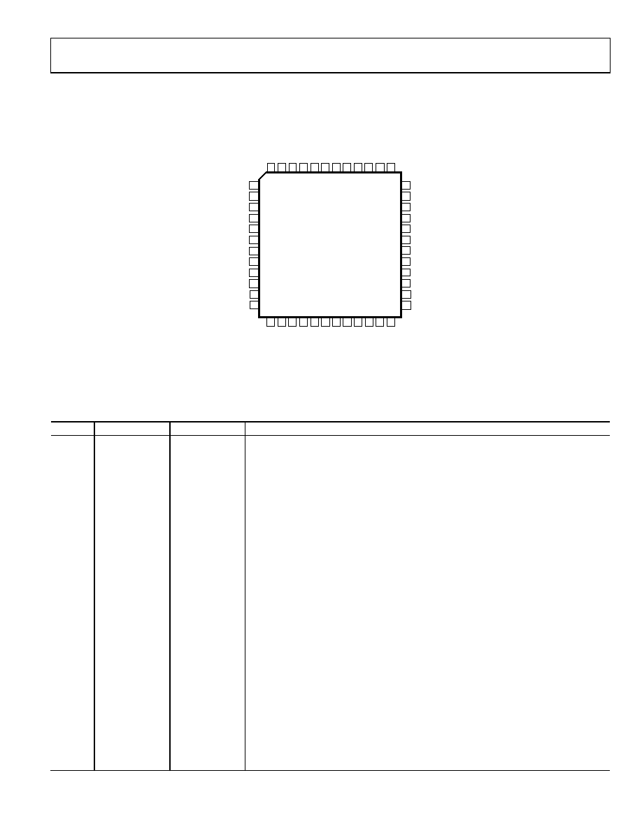
PIN CONFIGURATION AND FUNCTION DESCRIPTIONS
NC = NO CONNECT
AD1970
TOP VIEW
(Not to Scale)
DVDD
1
RESETB
2
DGND
3
DVDD
4
RSVD
5
DGND
GPIO1
GPIO0
XIN
XOUT
36
35
34
33
32
VOUT_OAMP
6
VIN_OAMP
7
AVDD
8
BTSC_OUT
9
AGND 10
VREF 11
FILTCAP 12
VID_PRES
MCLK
PLL_MODE1
PLL_MODE0
NC
31
30
29
28
27
VID_IN
PGND
26
25
AV
DD
13
AGND
14
V
O
UT_
IAMP
L
15
VIN
_
IA
M
P
L
16
V
O
UT_
IAMP
R
17
VIN
_
IA
M
P
R
18
CAP
LP
19
CAP
LN
20
CAP
RP
21
CAP
RN
22
PVD
D
23
PLL_LF
24
DGND
ADR0
ADR1
SC
L
SD
A
48
47
46
45
44
DIG_
IN_
E
N
LRCLK
BCLK
S
DATA
GPIO3
43
42
41
40
39
GPIO2
DV
DD
38
37
05500-002
Figure 2. Pin Configuration
Table 13. Pin Function Descriptions
Pin No.
Pin Name
Input/Output
Description
1
DVDD
Digital Power.
2
RESETB
IN
Reset—Active Low. After RESETB transitions from low to high, the AD1970 BTSC encoder
core goes through an initialization sequence where all registers are set to 0. The
initialization is completed after 1024 MCLK cycles. New values should not be written to
the control port until the initialization is complete.
3
DGND
Digital Ground.
4
DVDD
Digital Power. 3.3 V nominal.
5
RSVD
Reserved—Connect to DGND.
6
VOUT_OAMP
OUT
Output voltage of internal op amp to be used for BTSC output low pass filter.
7
VIN_OAMP
IN
Negative input of internal op amp to be used for BTSC output low pass filter.
8
AVDD
Analog Power.
9
BTSC_OUT
OUT
Encoded BTSC Output. The nominal output voltage for a 300 Hz, 0 dB mono input signal is
250 mV rms.
10
AGND
Analog Ground.
11
VREF
OUT
Connection for voltage reference noise reduction capacitor. The nominal VREF voltage is
1.5 V; the analog gain scales directly with the voltage on this pin. Any ac signal on this pin
causes distortion and therefore a large decoupling capacitor should be used to ensure the
voltage on VREF is clean.
12
FILTCAP
OUT
Connection for DAC noise reduction capacitor. A 10 F capacitor should be connected to
this pin to reduce the noise on an internal DAC biasing point to provide the highest
performance. It may not be necessary to connect this pin, depending on the quality of the
layout and grounding used in the application circuit.
13
AVDD
Analog Power. 3.3 V nominal. Bypass capacitors should be placed close to the pins and
connected directly to the analog ground plane.
14
AGND
Analog Ground.
15
VOUT_IAMPL
OUT
Output of internal op amp for left channel input amplifier.
16
VIN_IAMPL
IN
Negative input of internal op amp for left channel input amplifier.
17
VOUT_IAMPR
OUT
Output of internal op amp for right channel input amplifier.
相关PDF资料 |
PDF描述 |
|---|---|
| ADV7177KSZ | IC DAC VIDEO NTSC 3-CH 44MQFP |
| VI-24L-CU-S | CONVERTER MOD DC/DC 28V 200W |
| VI-24K-CU-S | CONVERTER MOD DC/DC 40V 200W |
| VI-24J-CU-S | CONVERTER MOD DC/DC 36V 200W |
| VI-241-CU-S | CONVERTER MOD DC/DC 12V 200W |
相关代理商/技术参数 |
参数描述 |
|---|---|
| AD1974 | 制造商:AD 制造商全称:Analog Devices 功能描述:4 ADC with PLL, 192 kHz, 24-Bit Codec |
| AD1974WBSTZ | 制造商:Analog Devices 功能描述: |
| AD1974WBSTZ-RL | 功能描述:ADC, Audio 24 bit 192k I2S 48-LQFP (7x7) 制造商:analog devices inc. 系列:- 包装:带卷(TR) 零件状态:有效 类型:ADC,音频 分辨率(位):24 b 采样率(每秒):192k 数据接口:I2S 电压源:模拟和数字 电压 - 电源:3 V ~ 3.6 V 工作温度:-40°C ~ 125°C 安装类型:表面贴装 封装/外壳:48-LQFP 供应商器件封装:48-LQFP(7x7) 标准包装:2,000 |
| AD1974YSTZ | 功能描述:IC ADC 4CH W/ON-CHIP PLL 48LQFP RoHS:是 类别:集成电路 (IC) >> 数据采集 - 模数转换器 系列:- 其它有关文件:TSA1204 View All Specifications 标准包装:1 系列:- 位数:12 采样率(每秒):20M 数据接口:并联 转换器数目:2 功率耗散(最大):155mW 电压电源:模拟和数字 工作温度:-40°C ~ 85°C 安装类型:表面贴装 封装/外壳:48-TQFP 供应商设备封装:48-TQFP(7x7) 包装:Digi-Reel® 输入数目和类型:4 个单端,单极;2 个差分,单极 产品目录页面:1156 (CN2011-ZH PDF) 其它名称:497-5435-6 |
| AD1974YSTZ-RL | 功能描述:IC CODEC 4CH ADC W/PLL 48-LQFP RoHS:是 类别:集成电路 (IC) >> 数据采集 - 模数转换器 系列:- 标准包装:1,000 系列:- 位数:16 采样率(每秒):45k 数据接口:串行 转换器数目:2 功率耗散(最大):315mW 电压电源:模拟和数字 工作温度:0°C ~ 70°C 安装类型:表面贴装 封装/外壳:28-SOIC(0.295",7.50mm 宽) 供应商设备封装:28-SOIC W 包装:带卷 (TR) 输入数目和类型:2 个单端,单极 |
发布紧急采购,3分钟左右您将得到回复。