参数资料
| 型号: | AD2S1205YSTZ |
| 厂商: | Analog Devices Inc |
| 文件页数: | 5/20页 |
| 文件大小: | 0K |
| 描述: | IC ADC R/D 12BIT W/OSC 44-LQFP |
| 标准包装: | 1 |
| 类型: | R/D 转换器 |
| 分辨率(位): | 12 b |
| 数据接口: | 串行,并联 |
| 电压电源: | 模拟和数字 |
| 电源电压: | 4.75 V ~ 5.25 V |
| 工作温度: | -40°C ~ 125°C |
| 安装类型: | 表面贴装 |
| 封装/外壳: | 44-LQFP |
| 供应商设备封装: | 44-LQFP(7x7) |
| 包装: | 托盘 |
AD2S1205
Rev. A | Page 13 of 20
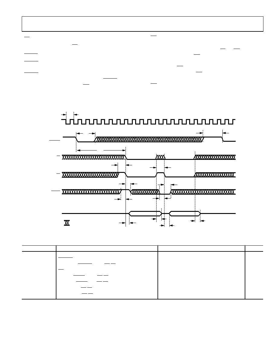
RD Input
CS Input
The 12-bit data bus lines are normally in a high impedance
state. The output buffer is enabled when CS and RD are held
low. A falling edge of the RD signal transfers data to the output
buffer. The selected data is made available to the bus to be read
within t6 of the RD pin going low. The data pins return to a high
impedance state when the RD pin returns to a high state within
t7. When reading data continuously, wait a minimum of t3 after
RD is released before reapplying it.
The device is enabled when CS is held low.
RDVEL Input
RDVEL input is used to select between the angular position
register and the angular velocity register, as shown in
RDVEL is held high to select the angular position register and
low to select the angular velocity register. The RDVEL pin must
be set (stable) at least t4 before the RD pin is pulled low.
06
33
9-
0
07
t3
t6
t7
fCLKIN
CLKIN
DATA
DON'T CARE
VELOCITY
POSITION
t2
SAMPLE
CS
RD
RDVEL
t1
t3
t5
t4
t5
t4
t7
t6
Figure 7. Parallel Port Read Timing
Table 6. Parallel Port Timing
Parameter
Description
Min
Typ
Max
Unit
fCLKIN
Frequency of clock input
6.144
8.192
10.24
MHz
t1
SAMPLE pulse width
2 × (1/fCLKIN) + 20
ns
t2
Delay from SAMPLE before RD/CS low
6 × (1/fCLKIN) + 20
ns
t3
RD pulse width
18
ns
t4
Set time RDVEL before RD/CS low
5
ns
t5
Hold time RDVEL after RD/CS low
7
ns
t6
Enable delay RD/CS low to data valid
30
ns
t7
Disable delay RD/CS low to data high-Z
18
ns
相关PDF资料 |
PDF描述 |
|---|---|
| AD2S1210ASTZ-RL7 | IC CONV R/D 10-16BIT OSC 48LQFP |
| AD2S44-UM18B | IC CONV SYNC/R-D 14BIT 2CH 32DIP |
| AD2S80AUD | IC R/D CONV TRACKING 40CDIP |
| AD2S83APZ-REEL | IC CONV R/D MONO VAR RES 44PLCC |
| AD2S90AP | IC R/D CONV 12BIT 20-PLCC |
相关代理商/技术参数 |
参数描述 |
|---|---|
| AD2S1210 | 制造商:AD 制造商全称:Analog Devices 功能描述:Variable Resolution, 10-Bit to 16-Bit R/D Converter with Reference Oscillator |
| AD2S1210ASTZ | 功能描述:IC CONV R/D 10-16BIT 48-LQFP RoHS:是 类别:集成电路 (IC) >> 数据采集 - ADCs/DAC - 专用型 系列:- 产品培训模块:Lead (SnPb) Finish for COTS Obsolescence Mitigation Program 标准包装:50 系列:- 类型:数据采集系统(DAS) 分辨率(位):16 b 采样率(每秒):21.94k 数据接口:MICROWIRE?,QSPI?,串行,SPI? 电压电源:模拟和数字 电源电压:1.8 V ~ 3.6 V 工作温度:-40°C ~ 85°C 安装类型:表面贴装 封装/外壳:40-WFQFN 裸露焊盘 供应商设备封装:40-TQFN-EP(6x6) 包装:托盘 |
| AD2S1210ASTZ-RL7 | 功能描述:IC CONV R/D 10-16BIT OSC 48LQFP RoHS:是 类别:集成电路 (IC) >> 数据采集 - ADCs/DAC - 专用型 系列:- 产品培训模块:Lead (SnPb) Finish for COTS Obsolescence Mitigation Program 标准包装:50 系列:- 类型:数据采集系统(DAS) 分辨率(位):16 b 采样率(每秒):21.94k 数据接口:MICROWIRE?,QSPI?,串行,SPI? 电压电源:模拟和数字 电源电压:1.8 V ~ 3.6 V 工作温度:-40°C ~ 85°C 安装类型:表面贴装 封装/外壳:40-WFQFN 裸露焊盘 供应商设备封装:40-TQFN-EP(6x6) 包装:托盘 |
| AD2S1210BSTZ | 功能描述:IC CONV R/D 10-16BIT 48-LQFP RoHS:是 类别:集成电路 (IC) >> 数据采集 - ADCs/DAC - 专用型 系列:- 产品培训模块:Lead (SnPb) Finish for COTS Obsolescence Mitigation Program 标准包装:50 系列:- 类型:数据采集系统(DAS) 分辨率(位):16 b 采样率(每秒):21.94k 数据接口:MICROWIRE?,QSPI?,串行,SPI? 电压电源:模拟和数字 电源电压:1.8 V ~ 3.6 V 工作温度:-40°C ~ 85°C 安装类型:表面贴装 封装/外壳:40-WFQFN 裸露焊盘 供应商设备封装:40-TQFN-EP(6x6) 包装:托盘 |
| AD2S1210BSTZ-DASSAULT | 制造商:Analog Devices 功能描述: |
发布紧急采购,3分钟左右您将得到回复。