- 您现在的位置:买卖IC网 > PDF目录11674 > AD2S90APZ (Analog Devices Inc)IC R/D CONV 12BIT 20-PLCC PDF资料下载
参数资料
| 型号: | AD2S90APZ |
| 厂商: | Analog Devices Inc |
| 文件页数: | 3/12页 |
| 文件大小: | 0K |
| 描述: | IC R/D CONV 12BIT 20-PLCC |
| 标准包装: | 1 |
| 类型: | R/D 转换器 |
| 输入类型: | 并联 |
| 输出类型: | 数字 |
| 接口: | 串行 |
| 电流 - 电源: | 10mA |
| 安装类型: | 表面贴装 |
| 封装/外壳: | 20-LCC(J 形引线) |
| 供应商设备封装: | 20-PLCC(9x9) |
| 包装: | 管件 |
| 产品目录页面: | 790 (CN2011-ZH PDF) |
AD2S90
REV. D
–11–
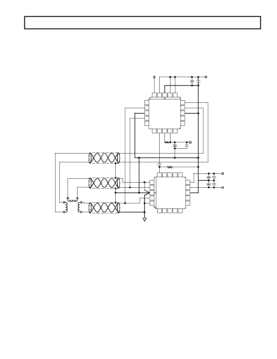
AD2S90/AD2S99 TYPICAL CONFIGURATION
Figure 21 shows a typical circuit configuration for the AD2S99
Oscillator and the AD2S90 Resolver-to-Digital Converter. The
maximum level of the SIN and COS input signals to the
AD2S90 should be 2 V rms
±10%. All the analog ground sig-
nals should be star connected to the AD2S90 AGND pin. If
shielded twisted pair cables are used for the resolver signals, the
shields should also be terminated at the AD2S90 AGND pin.
The SYNREF output of the AD2S99 should be connected to
the REF input pin of the AD2S90 via a 0.1
F capacitor with a
100 k
resistor to GND. This is to block out any dc offset in
the SYNREF signal. For more detailed information please refer
to the AD2S99 data sheet.
NC = NO CONNECT
NC
SIN
NC
DGND
COS
EXC
NC
AGND
NC
3
1
2
4
5
8
6
7
17
14
16
15
TOP VIEW
(Not to Scale)
AD2S99
F
BIAS
SEL1
V
SS
SEL2
V
SS
NC
SYNREF
NC
LOS
V
DD
19
3
1
2
20
4
5
8
6
7
12
13
9
11
10
18 17
14
16 15
4.7 F
0.1 F
COS
SIN
REF
S2
S4
S3
S1
R4
R2
RESOLVER
REF
COS
AGND
SIN
SIN LO
VDD
VSS
DGND
AD2S90
TOP VIEW
(Not to Scale)
0.1 F
100k
VDD
VSS
VDD
0.1 F
50k
4.7 F
0.1 F
4.7 F
VSS
SEL2 = GND
SEL1 = VSS
FOUT = 5kHz
COS LO
20 19
18
9
1011 1213
Figure 21. AD2S90 and AD2S99 Example Configuration
相关PDF资料 |
PDF描述 |
|---|---|
| 226990-3 | CONN JACK BNC RT/A 50OHM PCB AU |
| AD598JRZ | IC LVDT SGNL COND OSC/REF 20SOIC |
| 221185-2 | CONN PLUG BNC 75 OHM DUAL CRIMP |
| AD698APZ | IC LVDT SIGNAL COND 28-PLCC |
| 221185-8 | CONN PLUG BNC 75 OHM DUAL CRIMP |
相关代理商/技术参数 |
参数描述 |
|---|---|
| AD2S90APZ-MOOG | 制造商:Analog Devices 功能描述: |
| AD2S90APZ-RL7 | 功能描述:IC R/D CONV 12BIT 20-PLCC 制造商:analog devices inc. 系列:* 零件状态:在售 标准包装:250 |
| AD2S90-EB | 制造商:Analog Devices 功能描述:EVALUATION BOARD - Bulk |
| AD2S93 | 制造商:AD 制造商全称:Analog Devices 功能描述:Low Cost LVDT-to-Digital Converter |
| AD2S93AP | 制造商:AD 制造商全称:Analog Devices 功能描述:Low Cost LVDT-to-Digital Converter |
发布紧急采购,3分钟左右您将得到回复。