参数资料
| 型号: | AD5025BRUZ |
| 厂商: | Analog Devices Inc |
| 文件页数: | 27/28页 |
| 文件大小: | 0K |
| 描述: | IC DAC DUAL 12BIT SPI 14TSSOP |
| 产品培训模块: | Data Converter Fundamentals DAC Architectures |
| 标准包装: | 96 |
| 系列: | nanoDAC™ |
| 设置时间: | 5.8µs |
| 位数: | 12 |
| 数据接口: | 串行,SPI? |
| 转换器数目: | 2 |
| 电压电源: | 单电源 |
| 功率耗散(最大): | 13.5mW |
| 工作温度: | -40°C ~ 125°C |
| 安装类型: | 表面贴装 |
| 封装/外壳: | 14-TSSOP(0.173",4.40mm 宽) |
| 供应商设备封装: | 14-TSSOP |
| 包装: | 管件 |
| 输出数目和类型: | 2 电压,单极;2 电压,双极 |
| 采样率(每秒): | * |
| 产品目录页面: | 781 (CN2011-ZH PDF) |
第1页第2页第3页第4页第5页第6页第7页第8页第9页第10页第11页第12页第13页第14页第15页第16页第17页第18页第19页第20页第21页第22页第23页第24页第25页第26页当前第27页第28页
AD5025/AD5045/AD5065
Rev. 0 | Page 8 of 28
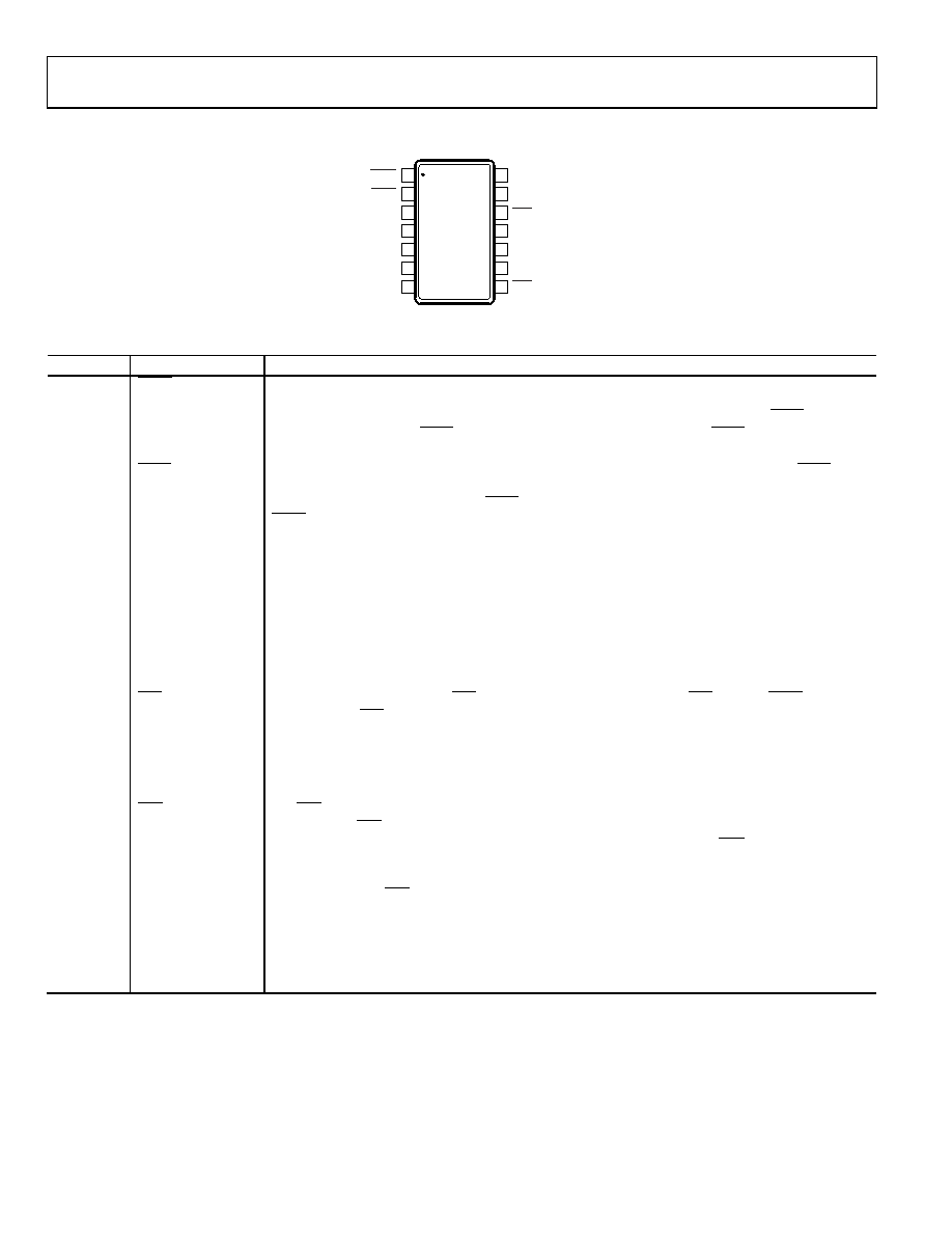
PIN CONFIGURATION AND FUNCTION DESCRIPTIONS
1
2
3
4
5
6
7
AD5025/
AD5045/
AD5065
VDD
VREFA
SDO
POR
VOUTA
14
13
12
11
10
9
8
DIN
GND
VOUTB
SCLK
TOP VIEW
(Not to Scale)
LDAC
CLR
PDL
SYNC
VREFB
06
84
4-
0
05
Figure 5. Pin Configuration
Table 6. Pin Function Descriptions
Pin No.
Mnemonic
Description
1
LDAC
Pulsing this pin low allows any or all DAC registers to be updated if the input registers have new data. This
allows all DAC outputs to simultaneously update. This pin can be tied permanently low in standalone
mode. When daisy-chain mode is enabled, this pin cannot be tied permanently low. The LDAC pin should
be used in asynchronous LDAC update mode, as shown in Figure 3, and the LDAC pin must be brought
high after pulsing. This allows all DAC outputs to simultaneously update.
2
SYNC
Active Low Control Input. This is the frame synchronization signal for the input data. When SYNC goes
low, it powers on the SCLK and DIN buffers and enables the input register. Data is transferred in on the
falling edges of the next 32 clocks. If SYNC is taken high before the 32nd falling edge, the rising edge of
SYNC acts as an interrupt and the write sequence is ignored by the device.
3
VDD
Power Supply Input. These parts can be operated from 4.5 V to 5.5 V, and the supply should be decoupled
with a 10 μF capacitor in parallel with a 0.1 μF capacitor to GND.
4
VREFA
DAC A Reference Input. This is the reference voltage input pin for DAC A.
5
VOUTA
Analog Output Voltage from DAC A. The output amplifier has rail-to-rail operation.
6
POR
Power-On Reset Pin. Tying this pin to GND powers up the part to 0 V. Tying this pin to VDD powers up
the part to midscale.
7
SDO
Serial Data Output. Can be used for daisy-chaining a number of these devices together or for reading
back the data in the shift register for diagnostic purposes. The serial data is transferred on the rising
edge of SCLK and is valid on the falling edge of the clock.
8
CLR
Asynchronous Clear Input. The CLR input is falling edge sensitive. When CLR is low, all LDAC pulses are
ignored. When CLR is activated, the input register and the DAC register are updated with the data
contained in the clear code register—zero, midscale, or full scale. Default setting clears the output to 0 V.
9
VREFB
DAC B Reference Input. This is the reference voltage input pin for DAC B.
10
VOUTB
Analog Output Voltage from DAC B. The output amplifier has rail-to-rail operation.
11
GND
Ground Reference Point for All Circuitry on the Part.
12
PDL
The PDL pin is used to ensure hardware shutdown lockout of the device under any circumstance. A
Logic 1 at the PLO pin causes the device to behave as normal. The user may successfully enter
software power-down over the serial interface while Logic 1 is applied to the PDL pin.
If a Logic 0 is applied to this pin, it ensures that the device cannot enter software power-down under
any circumstances. If the device had previously been placed in software power-down mode, a high-to-
low transition at the PDL pin causes the DAC(s) to exit power-down and output a voltage corresponding to
the previous code in the DAC register before the device entered software power-down.
13
DIN
Serial Data Input. This device has a 32-bit shift register. Data is clocked into the register on the falling
edge of the serial clock input.
14
SCLK
Serial Clock Input. Data is clocked into the input register on the falling edge of the serial clock input. Data
can be transferred at rates of up to 50 MHz.
相关PDF资料 |
PDF描述 |
|---|---|
| AD9760ARUZ | IC DAC 10BIT 125MSPS 28-TSSOP |
| AD5667RBRMZ-1 | IC DAC NANO 16BIT DUAL 10-MSOP |
| VE-262-MW-F1 | CONVERTER MOD DC/DC 15V 100W |
| VE-261-MW-F4 | CONVERTER MOD DC/DC 12V 100W |
| VE-261-MW-F3 | CONVERTER MOD DC/DC 12V 100W |
相关代理商/技术参数 |
参数描述 |
|---|---|
| AD5025BRUZ-REEL7 | 功能描述:IC DAC DUAL 12BIT SPI 14TSSOP RoHS:是 类别:集成电路 (IC) >> 数据采集 - 数模转换器 系列:nanoDAC™ 产品培训模块:LTC263x 12-, 10-, and 8-Bit VOUT DAC Family 特色产品:LTC2636 - Octal 12-/10-/8-Bit SPI VOUT DACs with 10ppm/°C Reference 标准包装:91 系列:- 设置时间:4µs 位数:10 数据接口:MICROWIRE?,串行,SPI? 转换器数目:8 电压电源:单电源 功率耗散(最大):2.7mW 工作温度:-40°C ~ 85°C 安装类型:表面贴装 封装/外壳:14-WFDFN 裸露焊盘 供应商设备封装:14-DFN-EP(4x3) 包装:管件 输出数目和类型:8 电压,单极 采样率(每秒):* |
| AD-5028S | 制造商:BOTHHAND 制造商全称:Bothhand USA, LP. 功能描述:ADSL LINE TRANSFORMER |
| AD50294 | 制造商:Analog Devices 功能描述: |
| AD50294-1 | 制造商:Analog Devices 功能描述: |
| AD503 | 制造商:INTERSIL 制造商全称:Intersil Corporation 功能描述:N-CHANNEL JFET |
发布紧急采购,3分钟左右您将得到回复。