- 您现在的位置:买卖IC网 > PDF目录1889 > AD5060YRJZ-1REEL7 (Analog Devices Inc)IC DAC 16BIT SPI/SRL SOT23-8 PDF资料下载
参数资料
| 型号: | AD5060YRJZ-1REEL7 |
| 厂商: | Analog Devices Inc |
| 文件页数: | 7/24页 |
| 文件大小: | 0K |
| 描述: | IC DAC 16BIT SPI/SRL SOT23-8 |
| 产品培训模块: | DAC Architectures |
| 标准包装: | 1 |
| 系列: | nanoDAC™ |
| 设置时间: | 4µs |
| 位数: | 16 |
| 数据接口: | DSP,MICROWIRE?,QSPI?,串行,SPI? |
| 转换器数目: | 1 |
| 电压电源: | 单电源 |
| 功率耗散(最大): | 6mW |
| 工作温度: | -40°C ~ 125°C |
| 安装类型: | 表面贴装 |
| 封装/外壳: | SOT-23-8 |
| 供应商设备封装: | SOT-23-8 |
| 包装: | 标准包装 |
| 输出数目和类型: | 1 电压,单极;1 电压,双极 |
| 采样率(每秒): | 250k |
| 产品目录页面: | 781 (CN2011-ZH PDF) |
| 其它名称: | AD5060YRJZ-1REEL7DKR |
AD5040/AD5060
Rev. A | Page 15 of 24
THEORY OF OPERATION
The AD5040/AD5060 are single 14-/16-bit, serial input, voltage
output DACs. The parts operate from supply voltages of 2.7 V
to 5.5 V. Data is written to the AD5060 in a 24-bit word format,
and to the AD5040 in a 16-bit word format, via a 3-wire serial
interface.
Both the AD5040 and AD5060 incorporate a power-on reset
circuit that ensures the DAC output powers up to a known out-
put state (midscale or zero-scale, see the Ordering Guide). The
devices also have a software power-down mode that reduces the
typical current consumption to less than 1 μa.
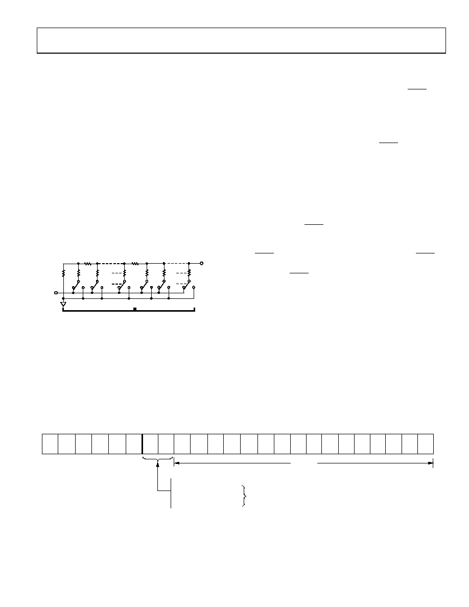
DAC ARCHITECTURE
The DAC architecture of the AD5060 consists of two matched
DAC sections. A simplified circuit diagram is shown in
Figure 40. The 4 MSBs of the 16-bit data-word are decoded to
drive 15 switches, E1 to E15. Each of these switches connects
1 of 15 matched resistors to either DACGND or the VREF
buffer
output. The remaining 12 bits of the data-word drive switches
S0 to S11 of a 12-bit voltage mode R-2R ladder network.
2R
04767
-027
S0
VREF
2R
S1
2R
S11
2R
E1
2R
E2
2R
E15
2R
VOUT
12-BIT R-2R LADDER
FOUR MSBs DECODED INTO
15 EQUAL SEGMENTS
Figure 40. AD5060 DAC Ladder Structure
REFERENCE BUFFER
The AD5040 andAD5060 operate with an external reference.
The reference input (VREF) has an input range of 2 V to
VDD 50 mV. This input voltage is then used to provide a
buffered reference for the DAC core.
SERIAL INTERFACE
The AD5060/AD5040 have a 3-wire serial interface (SYNC,
SCLK, and DIN), which is compatible with SPI, QSPI, and
MICROWIRE interface standards, as well as most DSPs.
shows a timing diagram of a typical AD5060 write
sequence.
The write sequence begins by bringing the SYNC line low. For
the AD5060, data from the DIN line is clocked into the 24-bit
shift register on the falling edge of SCLK. The serial clock
frequency can be as high as 30 MHz, making these parts
compatible with high speed DSPs. On the 24th falling clock
edge, the last data bit is clocked in and the programmed
function is executed (that is, a change in the DAC output or a
change in the mode of operation).
At this stage, the SYNC line can be kept low or be brought
high. In either case, it must be brought high for a minimum of
12 ns before the next write sequence so that a falling edge of
SYNC can initiate the next write sequence. Because the SYNC
buffer draws more current when VIH = 1.8 V than it does when
VIH = 0.8 V, SYNC should be idled low between write sequences
for an even lower power operation of the part. As previously
indicated, however, it must be brought high again just before
the next write sequence. The AD5040 requires 16 clock periods
to update the input shift register. On the 16th falling clock edge,
the last data bit is clocked in and the programmed function is
executed (that is, a change in the DAC output or a change in the
mode of operation).
Input Shift Register
The AD5060 input shift register is 24 bits wide; see Figure 41.
PD1 and PD0 are control bits that control the operating mode
of the part—normal mode or any one of three power-down
modes (see the Power-Down Modes section for more detail).
The next 16 bits are the data bits. These are transferred to the
DAC register on the 24th falling edge of SCLK.
DATA BITS
DB15 (MSB)
DB0 (LSB)
D15
D14
D13
D12
D11
D10
D9
D8
D7
D6
D5
D4
D3
D2
D1
D0
NORMAL OPERATION
1k
Ω TO GND
100k
Ω TO GND
3-STATE
POWER-DOWN MODES
0
1
0
1
0
1
04767
-028
0
PD1
PD0
Figure 41. AD5060 Input Register Content
相关PDF资料 |
PDF描述 |
|---|---|
| AD5061BRJZ-2500RL7 | IC DAC 16BIT SPI/SRL SOT23-8 |
| AD5062BRJZ-2REEL7 | IC DAC 16BIT 2.7-5.5V SOT23-8 |
| AD5063BRMZ-1-REEL7 | IC DAC 16BIT 2.7-5.5V 10MSOP |
| AD5064BRUZ-1REEL7 | IC DAC 16BIT 4CH BUF OUT 14TSSOP |
| AD5065ARUZ | IC DAC 16BIT SPI 14TSSOP |
相关代理商/技术参数 |
参数描述 |
|---|---|
| AD5061 | 制造商:AD 制造商全称:Analog Devices 功能描述:Full Accurate 14/16 Bit Vout nanoDac Buffered, 3V/5V, Sot 23 |
| AD50611-1 | 制造商:Rochester Electronics LLC 功能描述:- Bulk |
| AD5061BRJZ-1 | 制造商:Analog Devices 功能描述:DAC SGL R-2R 16BIT 8PIN SOT-23 - Bulk |
| AD5061BRJZ-1500RL7 | 功能描述:IC DAC 16BIT SPI/SRL SOT23-8 RoHS:是 类别:集成电路 (IC) >> 数据采集 - 数模转换器 系列:nanoDAC™ 产品培训模块:LTC263x 12-, 10-, and 8-Bit VOUT DAC Family 特色产品:LTC2636 - Octal 12-/10-/8-Bit SPI VOUT DACs with 10ppm/°C Reference 标准包装:91 系列:- 设置时间:4µs 位数:10 数据接口:MICROWIRE?,串行,SPI? 转换器数目:8 电压电源:单电源 功率耗散(最大):2.7mW 工作温度:-40°C ~ 85°C 安装类型:表面贴装 封装/外壳:14-WFDFN 裸露焊盘 供应商设备封装:14-DFN-EP(4x3) 包装:管件 输出数目和类型:8 电压,单极 采样率(每秒):* |
| AD5061BRJZ-1REEL7 | 功能描述:IC DAC 16BIT SPI/SRL SOT23-8 RoHS:是 类别:集成电路 (IC) >> 数据采集 - 数模转换器 系列:nanoDAC™ 产品培训模块:LTC263x 12-, 10-, and 8-Bit VOUT DAC Family 特色产品:LTC2636 - Octal 12-/10-/8-Bit SPI VOUT DACs with 10ppm/°C Reference 标准包装:91 系列:- 设置时间:4µs 位数:10 数据接口:MICROWIRE?,串行,SPI? 转换器数目:8 电压电源:单电源 功率耗散(最大):2.7mW 工作温度:-40°C ~ 85°C 安装类型:表面贴装 封装/外壳:14-WFDFN 裸露焊盘 供应商设备封装:14-DFN-EP(4x3) 包装:管件 输出数目和类型:8 电压,单极 采样率(每秒):* |
发布紧急采购,3分钟左右您将得到回复。