- 您现在的位置:买卖IC网 > PDF目录8981 > AD5062BRJZ-2500RL7 (Analog Devices Inc)IC DAC 16BIT 2.7-5.5V SOT23-8 PDF资料下载
参数资料
| 型号: | AD5062BRJZ-2500RL7 |
| 厂商: | Analog Devices Inc |
| 文件页数: | 8/20页 |
| 文件大小: | 0K |
| 描述: | IC DAC 16BIT 2.7-5.5V SOT23-8 |
| 产品培训模块: | Data Converter Fundamentals DAC Architectures |
| 标准包装: | 1 |
| 系列: | nanoDAC™ |
| 设置时间: | 4µs |
| 位数: | 16 |
| 数据接口: | DSP,MICROWIRE?,QSPI?,串行,SPI? |
| 转换器数目: | 1 |
| 电压电源: | 单电源 |
| 工作温度: | -40°C ~ 85°C |
| 安装类型: | 表面贴装 |
| 封装/外壳: | SOT-23-8 |
| 供应商设备封装: | SOT-23-8 |
| 包装: | 标准包装 |
| 输出数目和类型: | 1 电压,单极;1 电压,双极 |
| 采样率(每秒): | 1.3M |
| 其它名称: | AD5062BRJZ-2500RL7DKR |
AD5062
Rev. A | Page 16 of 20
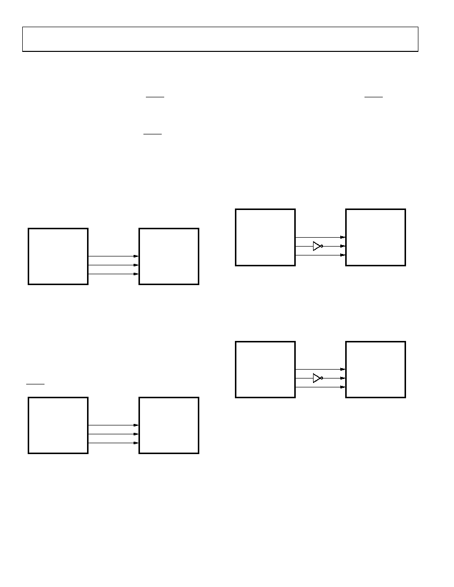
AD5062 to 68HC11/68L11 Interface
Figure 38 shows a serial interface between the AD5062 and the
68HC11/68L11 microcontroller. SCK of the 68HC11/68L11
drives the SCLK pin of the AD5062, while the MOSI output
drives the serial data line of the DAC. The SYNC signal is
derived from a port line (PC7). The setup conditions for correct
operation of this interface require that the 68HC11/68L11 be
configured so that its CPOL bit is 0 and its CPHA bit is 1. When
data is being transmitted to the DAC, the SYNC line is taken
low (PC7). When the 68HC11/68L11 is configured where its
CPOL bit is 0 and its CPHA bit is 1, data appearing on the
MOSI output is valid on the falling edge of SCK. Serial data
from the 68HC11/68L11 is transmitted in 8-bit bytes with only
eight falling clock edges occurring in the transmit cycle. Data is
transmitted MSB first. In order to load data to the AD5062,
PC7 is left low after the first eight bits are transferred, and a
second serial write operation is performed to the DAC, and PC7
is taken high at the end of this procedure.
AD50621
1ADDITIONAL PINS OMITTED FOR CLARITY
PC7
SCK
MOSI
SYNC
SCLK
DIN
04766-032
68HC11/
68L111
Figure 38. AD5062 to 68HC11/68L11 Interface
AD5062 to Blackfin ADSP-BF53x Interface
Figure 39 shows a serial interface between the AD5062 and the
Blackfin ADSP-53x microprocessor. The ADSP-BF53x proces-
sor family incorporates two dual-channel synchronous serial
ports, SPORT1 and SPORT0, for serial and multiprocessor
communications. Using SPORT0 to connect to the AD5062,
the setup for the interface is: DT0PRI drives the SDIN pin of
the AD5062, while TSCLK0 drives the SCLK of the part; the
SYNC is driven from TFS0.
ADSP-BF53x1
AD50621
1ADDITIONAL PINS OMITTED FOR CLARITY
DT0PRI
TSCLK0
TFS0
DIN
SCLK
SYNC
04766-033
Figure 39. AD5062 to Blackfin ADSP-BF53x Interface
AD5062 to 80C51/80L51 Interface
Figure 40 shows a serial interface between the AD5062 and the
80C51/80L51 microcontroller. The setup for the interface is:
TxD of the 80C51/80L51 drives SCLK of the AD5062 while
RxD drives the serial data line of the part. The SYNC signal is
again derived from a bit-programmable pin on the port. In this
case, Port Line P3.3 is used. When data is to be transmitted to
the AD5062, P3.3 is taken low. The 80C51/80L51 transmits data
only in 8-bit bytes; thus only eight falling clock edges occur in
the transmit cycle. To load data to the DAC, P3.3 is left low after
the first eight bits are transmitted, and a second write cycle is
initiated to transmit the second byte of data. P3.3 is taken high
following the completion of this cycle. The 80C51/80L51
outputs the serial data in a format that has the LSB first. The
AD5062 requires its data with the MSB as the first bit received;
the 80C51/80L51 transmit routine should take this into account.
80C51/80L511
AD50621
1ADDITIONAL PINS OMITTED FOR CLARITY
P3.3
TxD
RxD
SYNC
SCLK
DIN
04766-034
Figure 40. AD5062 to 80C51/80L51 Interface
AD5062 to MICROWIRE Interface
Figure 41 shows an interface between the AD5062 and any
MICROWIRE-compatible device. Serial data is shifted out on
the falling edge of the serial clock and is clocked into the
AD5062 on the rising edge of the SK.
MICROWIRE1
AD50621
1ADDITIONAL PINS OMITTED FOR CLARITY
CS
SK
SO
SYNC
SCLK
DIN
04766-035
Figure 41. AD5062 to MICROWIRE Interface
相关PDF资料 |
PDF描述 |
|---|---|
| ICS843023AGILFT | IC CLK GENERATOR LVPECL 8-TSSOP |
| AD5063BRMZ | IC DAC 16BIT 2.7-5.5V 10-MSOP |
| AD5063BRMZ-1 | IC DAC 16BIT 2.7-5.5V 10MSOP |
| VE-J0P-MZ-F4 | CONVERTER MOD DC/DC 13.8V 25W |
| VI-B0T-MY-F2 | CONVERTER MOD DC/DC 6.5V 50W |
相关代理商/技术参数 |
参数描述 |
|---|---|
| AD5062BRJZ-2REEL7 | 功能描述:IC DAC 16BIT 2.7-5.5V SOT23-8 RoHS:是 类别:集成电路 (IC) >> 数据采集 - 数模转换器 系列:nanoDAC™ 标准包装:47 系列:- 设置时间:2µs 位数:14 数据接口:并联 转换器数目:1 电压电源:单电源 功率耗散(最大):55µW 工作温度:-40°C ~ 85°C 安装类型:表面贴装 封装/外壳:28-SSOP(0.209",5.30mm 宽) 供应商设备封装:28-SSOP 包装:管件 输出数目和类型:1 电流,单极;1 电流,双极 采样率(每秒):* |
| AD5063 | 制造商:AD 制造商全称:Analog Devices 功能描述:Full Accurate 14/16 Bit Vout nanoDac Buffered, 3V/5V, Sot 23 |
| AD5063_09 | 制造商:AD 制造商全称:Analog Devices 功能描述:Fully Accurate 16-Bit VOUT nanoDAC SPI Interface 2.7 V to 5.5 V in an MSOP |
| AD50631 | 制造商:AD 制造商全称:Analog Devices 功能描述:Fully Accurate, 16-Bit, Unbuffered VOUT, Quad SPI Interface, 2.7 V to 5.5 V nanoDAC in a TSSOP |
| AD5063BRM-1 | 制造商:AD 制造商全称:Analog Devices 功能描述:Full Accurate 16 Bit Vout nanoDac, 2.7V- 5.5V, in a Sot 23 |
发布紧急采购,3分钟左右您将得到回复。