- 您现在的位置:买卖IC网 > PDF目录8889 > AD5064ARUZ-1 (Analog Devices Inc)IC DAC 16BIT 4CH BUF OUT 14TSSOP PDF资料下载
参数资料
| 型号: | AD5064ARUZ-1 |
| 厂商: | Analog Devices Inc |
| 文件页数: | 28/28页 |
| 文件大小: | 0K |
| 描述: | IC DAC 16BIT 4CH BUF OUT 14TSSOP |
| 产品培训模块: | Data Converter Fundamentals DAC Architectures |
| 标准包装: | 1 |
| 系列: | nanoDAC™ |
| 设置时间: | 5.8µs |
| 位数: | 16 |
| 数据接口: | 串行 |
| 转换器数目: | 4 |
| 电压电源: | 单电源 |
| 功率耗散(最大): | 30mW |
| 工作温度: | -40°C ~ 125°C |
| 安装类型: | 表面贴装 |
| 封装/外壳: | 14-TSSOP(0.173",4.40mm 宽) |
| 供应商设备封装: | 14-TSSOP |
| 包装: | 管件 |
| 输出数目和类型: | 4 电压,双极 |
| 采样率(每秒): | 125k |
| 产品目录页面: | 781 (CN2011-ZH PDF) |
第1页第2页第3页第4页第5页第6页第7页第8页第9页第10页第11页第12页第13页第14页第15页第16页第17页第18页第19页第20页第21页第22页第23页第24页第25页第26页第27页当前第28页
Data Sheet
AD5024/AD5044/AD5064
Rev. F | Page 9 of 28
VOUTA
VREFA
VREFB
VOUTC
POR
DIN
GND
VOUTB
VOUTD
VREFC
VREFD
SCLK
CLR
VDD
LDAC
SYNC
TOP VIEW
(Not to Scale)
1
2
3
4
5
6
7
8
AD5024/
AD5044/
AD5064
16
15
14
13
12
11
10
9
06803-
005
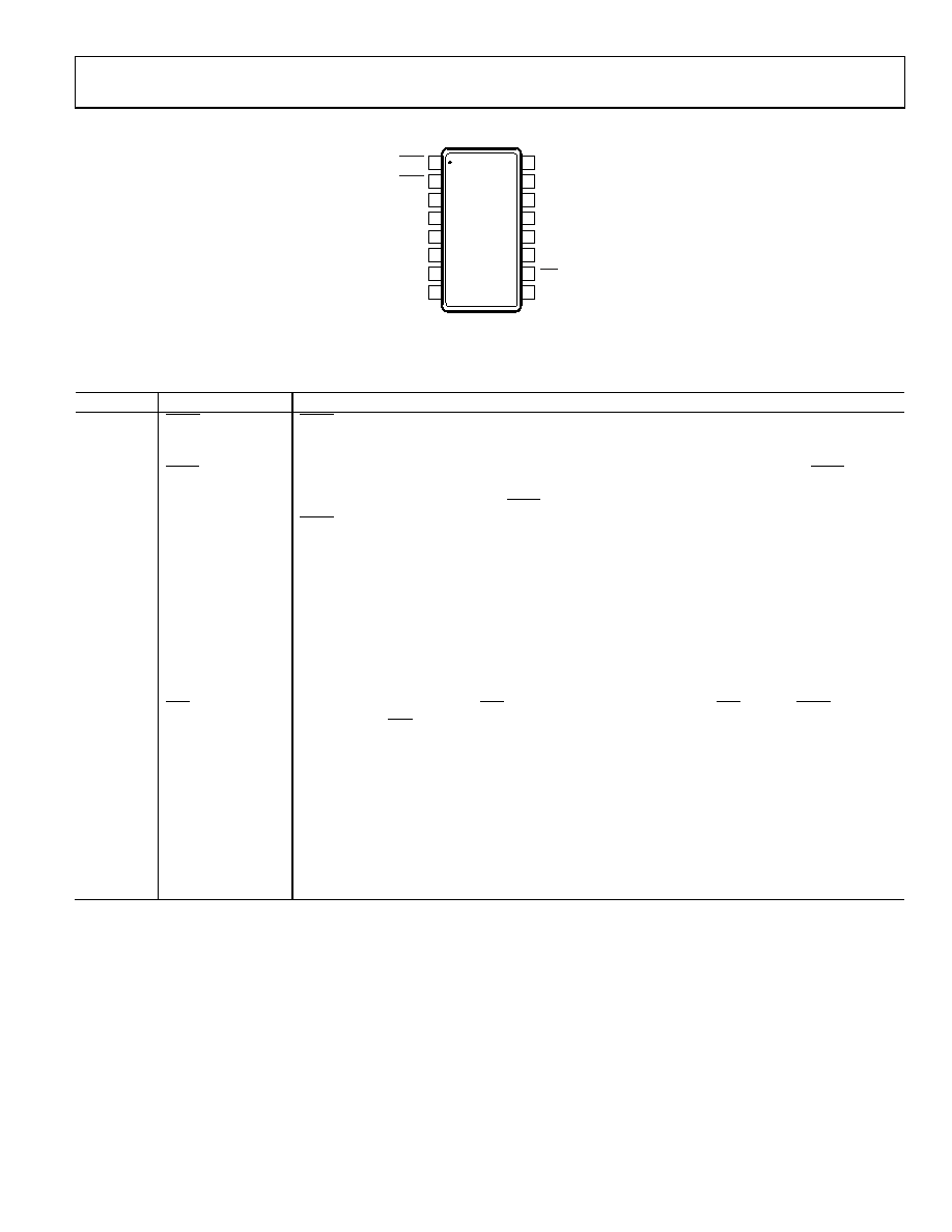
Figure 7. 16-Lead TSSOP (RU-16) Pin Configuration
Table 7. Pin Function Descriptions
Pin No.
Mnemonic
Description
1
LDAC
LDAC can be operated in two modes, asynchronously and synchronously, as shown in Figure 4. Pulsing
this pin low allows any or all DAC registers to be updated if the input registers have new data. This allows
all DAC outputs to simultaneously update. This pin can also be tied permanently low in standalone mode.
2
SYNC
Active Low Control Input. This is the frame synchronization signal for the input data. When SYNC goes
low, it powers on the SCLK and DIN buffers and enables the shift register. Data is transferred in on the
falling edges of the next 32 clocks. If SYNC is taken high before the 32nd falling edge, the rising edge of
SYNC acts as an interrupt and the write sequence is ignored by the device.
3
VDD
Power Supply Input. These parts can be operated from 4.5 V to 5.5 V, and the supply should be decoupled
with a 10 F capacitor in parallel with a 0.1 F capacitor to GND.
4
VREFB
DAC B Reference Input. This is the reference voltage input pin for DAC B.
5
VREFA
DAC A Reference Input. This is the reference voltage input pin for DAC A.
6
VOUTA
Analog Output Voltage from DAC A. The output amplifier has rail-to-rail operation.
7
VOUTC
Analog Output Voltage from DAC C. The output amplifier has rail-to-rail operation.
8
POR
Power-On Reset. Tying this pin to GND powers up the part to 0 V. Tying this pin to VDD powers up the
part to midscale.
9
VREFC
DAC C Reference Input. This is the reference voltage input pin for DAC C.
10
CLR
Asynchronous Clear Input. The CLR input is falling edge sensitive. When CLR is low, all LDAC pulses are
ignored. When CLR is activated, the input register and the DAC register are updated with the data
contained in the clear code register—zero, midscale, or full scale. Default setting clears the output to 0 V.
11
VREFD
DAC D Reference Input. This is the reference voltage input pin for DAC D.
12
VOUTD
Analog Output Voltage from DAC D. The output amplifier has rail-to-rail operation.
13
VOUTB
Analog Output Voltage from DAC B. The output amplifier has rail-to-rail operation.
14
GND
Ground Reference Point for All Circuitry on the Part.
15
DIN
Serial Data Input. This device has a 32-bit shift register. Data is clocked into the shift register on the
falling edge of the serial clock input.
16
SCLK
Serial Clock Input. Data is clocked into the shift register on the falling edge of the serial clock input. Data
can be transferred at rates of up to 50 MHz.
相关PDF资料 |
PDF描述 |
|---|---|
| MS27473T10B99PLC | CONN HSG PLUG 7POS STRGHT PINS |
| D38999/26KF32SC | CONN PLUG 32POS STRAIGHT W/SCKT |
| AD5066BRUZ | IC DAC 16BIT 2.7-5.5V 16TSSOP |
| VI-21N-MW-F3 | CONVERTER MOD DC/DC 18.5V 100W |
| VI-21N-MW-F2 | CONVERTER MOD DC/DC 18.5V 100W |
相关代理商/技术参数 |
参数描述 |
|---|---|
| AD5064ARUZ-1REEL7 | 功能描述:IC DAC 16BIT 4CH BUF OUT 14TSSOP RoHS:是 类别:集成电路 (IC) >> 数据采集 - 数模转换器 系列:nanoDAC™ 产品培训模块:Data Converter Fundamentals DAC Architectures 标准包装:750 系列:- 设置时间:7µs 位数:16 数据接口:并联 转换器数目:1 电压电源:双 ± 功率耗散(最大):100mW 工作温度:0°C ~ 70°C 安装类型:表面贴装 封装/外壳:28-LCC(J 形引线) 供应商设备封装:28-PLCC(11.51x11.51) 包装:带卷 (TR) 输出数目和类型:1 电压,单极;1 电压,双极 采样率(每秒):143k |
| AD5064BRUZ | 功能描述:IC DAC 16BIT 4CH BUF OUT 16TSSOP RoHS:是 类别:集成电路 (IC) >> 数据采集 - 数模转换器 系列:nanoDAC™ 产品培训模块:Lead (SnPb) Finish for COTS Obsolescence Mitigation Program 标准包装:50 系列:- 设置时间:4µs 位数:12 数据接口:串行 转换器数目:2 电压电源:单电源 功率耗散(最大):- 工作温度:-40°C ~ 85°C 安装类型:表面贴装 封装/外壳:8-TSSOP,8-MSOP(0.118",3.00mm 宽) 供应商设备封装:8-uMAX 包装:管件 输出数目和类型:2 电压,单极 采样率(每秒):* 产品目录页面:1398 (CN2011-ZH PDF) |
| AD5064BRUZ-1 | 功能描述:IC DAC 16BIT 4CH BUF OUT 14TSSOP RoHS:是 类别:集成电路 (IC) >> 数据采集 - 数模转换器 系列:nanoDAC™ 产品培训模块:Lead (SnPb) Finish for COTS Obsolescence Mitigation Program 标准包装:50 系列:- 设置时间:4µs 位数:12 数据接口:串行 转换器数目:2 电压电源:单电源 功率耗散(最大):- 工作温度:-40°C ~ 85°C 安装类型:表面贴装 封装/外壳:8-TSSOP,8-MSOP(0.118",3.00mm 宽) 供应商设备封装:8-uMAX 包装:管件 输出数目和类型:2 电压,单极 采样率(每秒):* 产品目录页面:1398 (CN2011-ZH PDF) |
| AD5064BRUZ-1REEL7 | 功能描述:IC DAC 16BIT 4CH BUF OUT 14TSSOP RoHS:是 类别:集成电路 (IC) >> 数据采集 - 数模转换器 系列:nanoDAC™ 产品培训模块:Data Converter Fundamentals DAC Architectures 标准包装:750 系列:- 设置时间:7µs 位数:16 数据接口:并联 转换器数目:1 电压电源:双 ± 功率耗散(最大):100mW 工作温度:0°C ~ 70°C 安装类型:表面贴装 封装/外壳:28-LCC(J 形引线) 供应商设备封装:28-PLCC(11.51x11.51) 包装:带卷 (TR) 输出数目和类型:1 电压,单极;1 电压,双极 采样率(每秒):143k |
| AD5064BRUZ-REEL7 | 功能描述:IC DAC 16BIT 4CH BUF OUT 16TSSOP RoHS:是 类别:集成电路 (IC) >> 数据采集 - 数模转换器 系列:nanoDAC™ 产品培训模块:Data Converter Fundamentals DAC Architectures 标准包装:750 系列:- 设置时间:7µs 位数:16 数据接口:并联 转换器数目:1 电压电源:双 ± 功率耗散(最大):100mW 工作温度:0°C ~ 70°C 安装类型:表面贴装 封装/外壳:28-LCC(J 形引线) 供应商设备封装:28-PLCC(11.51x11.51) 包装:带卷 (TR) 输出数目和类型:1 电压,单极;1 电压,双极 采样率(每秒):143k |
发布紧急采购,3分钟左右您将得到回复。