- 您现在的位置:买卖IC网 > PDF目录9302 > AD5160BRJZ100-R2 (Analog Devices Inc)IC DGTL POT 100K SPI SOT23-8 PDF资料下载
参数资料
| 型号: | AD5160BRJZ100-R2 |
| 厂商: | Analog Devices Inc |
| 文件页数: | 7/16页 |
| 文件大小: | 0K |
| 描述: | IC DGTL POT 100K SPI SOT23-8 |
| 标准包装: | 1 |
| 接片: | 256 |
| 电阻(欧姆): | 100k |
| 电路数: | 1 |
| 温度系数: | 标准值 45 ppm/°C |
| 存储器类型: | 易失 |
| 接口: | 3 线串行(芯片选择) |
| 电源电压: | 2.7 V ~ 5.5 V |
| 工作温度: | -40°C ~ 125°C |
| 安装类型: | 表面贴装 |
| 封装/外壳: | SOT-23-8 |
| 供应商设备封装: | SOT-23-8 |
| 包装: | 剪切带 (CT) |
| 其它名称: | AD5160BRJZ100R2CT |
AD5160
Rev. B | Page 15 of 1
6
PROGRAMMING THE POTENTIOMETER DIVIDER
Voltage Output Operation
The digital potentiometer easily generates a voltage divider at
wiper-to-B and wiper-to-A proportional to the input voltage at
A-to-B. Unlike the polarity of VDD to GND, which must be
positive, voltage across A to B, W to A, and W to B can be at
either polarity.
If ignoring the effect of the wiper resistance for approximation,
connecting the A terminal to 5 V and the B terminal to ground
produces an output voltage at the wiper-to-B starting at 0 V up
to 1 LSB less than 5 V. Each LSB of voltage is equal to the
voltage applied across Terminal A and Terminal B divided by
the 256 positions of the potentiometer divider. The general
equation defining the output voltage at VW with respect to
ground for any valid input voltage applied to Terminal A and
Terminal B is
B
A
W
V
D
V
256
)
(
+
=
D
256
(3)
For a more accurate calculation, which includes the effect of
wiper resistance, VW can be found as
B
WA
A
WB
W
V
D
R
V
D
R
D
V
256
)
(
256
)
(
)
(
+
=
(4)
Operation of the digital potentiometer in the divider mode
results in a more accurate operation over temperature. Unlike
the rheostat mode, the output voltage is dependent mainly on
the ratio of the internal resistors (RWA and RWB) and not the
absolute values. Therefore, the temperature drift reduces to
15 ppm/°C.
SPI-COMPATIBLE 3-WIRE SERIAL BUS
The AD5160 contains a 3-wire SPI-compatible digital interface
(SDI, CS, and CLK). The 8-bit serial word must be loaded MSB
first. The format of the word is shown in
.
The positive-edge sensitive CLK input requires clean transitions
to avoid clocking incorrect data into the serial input register.
Standard logic families work well. If mechanical switches are
used for product evaluation, they should be debounced by a
flip-flop or other suitable means. When CS is low, the clock
loads data into the serial register on each positive clock edge
(see
).
The data setup and data hold times in the specification table
determine the valid timing requirements. The AD5160 uses an
8-bit serial input data register word that is transferred to the
internal RDAC register when the CS line returns to logic high.
Extra MSB bits are ignored.
ESD PROTECTION
All digital inputs are protected with a series input resistor and
parallel Zener ESD structures are shown in Figure 40 and
Figure 41. This applies to SDI, CLK, and CS, which are the
digital input pins.
LOGIC
340
GND
Figure 40. ESD Protection of Digital Pins
A,B,W
GND
Figure 41. ESD Protection of Resistor Terminals
POWER-UP SEQUENCE
Because the ESD protection diodes limit the voltage compliance
at the A, B, and W terminals, it is important to power VDD/GND
before applying any voltage to the A, B, and W terminals;
otherwise, the diode forward biases such that VDD is powered
unintentionally and may affect the rest of the user’s circuit. The
ideal power-up sequence is in the following order: GND, VDD,
digital inputs, and then VA/B/W. The relative order of powering
VA, VB, VW, and the digital inputs is not important as long as
they are powered after VDD/GND.
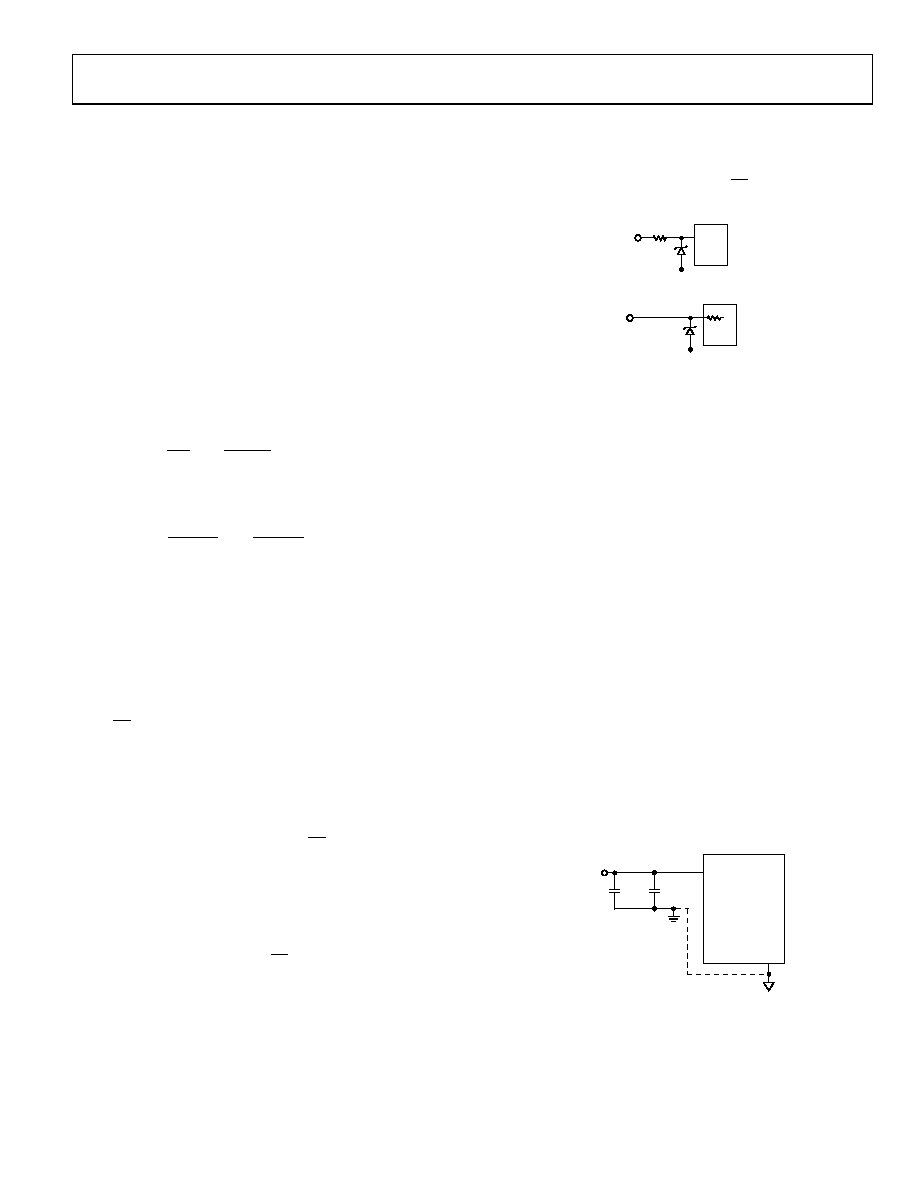
LAYOUT AND POWER SUPPLY BYPASSING
It is a good practice to employ compact, minimum lead length
layout design. Keep the leads to the inputs as direct as possible
with a minimum conductor length. Ground paths should have
low resistance and low inductance.
Similarly, it is also a good practice to bypass the power supplies
with quality capacitors for optimum stability. Bypass supply
leads to the device with disc or chip ceramic capacitors of
0.01 μF to 0.1 μF. To minimize any transient disturbance and
low frequency ripple, apply low ESR 1 μF to 10 μF tantalum or
electrolytic capacitors at the supplies (see Figure 42). To
minimize the ground bounce, join the digital ground remotely
to the analog ground at a single point.
AD5160
VDD
C1
C3
GND
10
μF
0.1
μF
+
VDD
Figure 42. Power Supply Bypassing
相关PDF资料 |
PDF描述 |
|---|---|
| VE-B63-MY-F1 | CONVERTER MOD DC/DC 24V 50W |
| VE-B62-MY-F3 | CONVERTER MOD DC/DC 15V 50W |
| VE-B62-MY-F2 | CONVERTER MOD DC/DC 15V 50W |
| VE-B62-MY-F1 | CONVERTER MOD DC/DC 15V 50W |
| AD5170BRMZ2.5 | IC POT DGTL 2.5K 256POS 10-MSOP |
相关代理商/技术参数 |
参数描述 |
|---|---|
| AD5160BRJZ100-R2 | 制造商:Analog Devices 功能描述:IC 8-BIT DIGITAL POT |
| AD5160BRJZ100-R22 | 制造商:AD 制造商全称:Analog Devices 功能描述:256-Position SPI-Compatible Digital Potentiometer |
| AD5160BRJZ100-RL7 | 功能描述:IC POT DGTL SPI 256POS SOT23-8 RoHS:是 类别:集成电路 (IC) >> 数据采集 - 数字电位器 系列:- 标准包装:3,300 系列:WiperLock™ 接片:257 电阻(欧姆):100k 电路数:1 温度系数:标准值 150 ppm/°C 存储器类型:易失 接口:3 线 SPI(芯片选择) 电源电压:1.8 V ~ 5.5 V 工作温度:-40°C ~ 125°C 安装类型:表面贴装 封装/外壳:8-VDFN 裸露焊盘 供应商设备封装:8-DFN-EP(3x3) 包装:带卷 (TR) |
| AD5160BRJZ100-RL72 | 制造商:AD 制造商全称:Analog Devices 功能描述:256-Position SPI-Compatible Digital Potentiometer |
| AD5160BRJZ10-R2 | 功能描述:IC POT DGTL SPI 256POS SOT23-8 RoHS:是 类别:集成电路 (IC) >> 数据采集 - 数字电位器 系列:- 标准包装:3,300 系列:WiperLock™ 接片:257 电阻(欧姆):100k 电路数:1 温度系数:标准值 150 ppm/°C 存储器类型:易失 接口:3 线 SPI(芯片选择) 电源电压:1.8 V ~ 5.5 V 工作温度:-40°C ~ 125°C 安装类型:表面贴装 封装/外壳:8-VDFN 裸露焊盘 供应商设备封装:8-DFN-EP(3x3) 包装:带卷 (TR) |
发布紧急采购,3分钟左右您将得到回复。