- 您现在的位置:买卖IC网 > PDF目录9310 > AD5161BRM10-RL7 (Analog Devices Inc)IC DGTL POT SPI 256POS 10-MSOP PDF资料下载
参数资料
| 型号: | AD5161BRM10-RL7 |
| 厂商: | Analog Devices Inc |
| 文件页数: | 9/20页 |
| 文件大小: | 0K |
| 描述: | IC DGTL POT SPI 256POS 10-MSOP |
| 标准包装: | 1,000 |
| 接片: | 256 |
| 电阻(欧姆): | 10k |
| 电路数: | 1 |
| 温度系数: | 标准值 45 ppm/°C |
| 存储器类型: | 易失 |
| 接口: | I²C,SPI |
| 电源电压: | 2.7 V ~ 5.5 V |
| 工作温度: | -40°C ~ 125°C |
| 安装类型: | 表面贴装 |
| 封装/外壳: | 10-TFSOP,10-MSOP(0.118",3.00mm 宽) |
| 供应商设备封装: | 10-MSOP |
| 包装: | 带卷 (TR) |
Data Sheet
AD5161
Rev. B | Page 17 of 20
The slave whose address corresponds to the transmitted
address responds by pulling the SDA line low during the
ninth clock pulse (this is termed the acknowledge bit). At
this stage, all other devices on the bus remain idle while the
selected device waits for data to be written to or read from
its serial register. If the R/W bit is high, the master will read
from the slave device. On the other hand, if the R/W bit is
low, the master will write to the slave device.
2. A write operation contains an extra instruction byte that a
read operation does not contain. Such an instruction byte
in write mode follows the slave address byte. The first bit
(MSB) of the instruction byte is a don’t care.
The second MSB, RS, is the midscale reset. A logic high on
this bit moves the wiper to the center tap where RWA = RWB.
This feature effectively writes over the contents of the
register, and thus, when taken out of reset mode, the
RDAC will remain at midscale.
The third MSB, SD, is a shutdown bit. A logic high causes
an open circuit at terminal A while shorting the wiper to
terminal B. This operation yields almost 0 in rheostat
mode or 0 V in potentiometer mode. It is important to
note that the shutdown operation does not disturb the
contents of the register. When brought out of shutdown,
the previous setting will be applied to the RDAC. Also,
during shutdown, new settings can be programmed. When
the part is returned from shutdown, the corresponding VR
setting will be applied to the RDAC.
The remainder of the bits in the instruction byte are don’t
cares (see Table 7).
3. After acknowledging the instruction byte, the last byte in
write mode is the data byte. Data is transmitted over the
serial bus in sequences of nine clock pulses (eight data bits
followed by an acknowledge bit). The transitions on the
SDA line must occur during the low period of SCL and
remain stable during the high period of SCL (see Table 7).
4. In the read mode, the data byte follows immediately after
the acknowledgment of the slave address byte. Data is
transmitted over the serial bus in sequences of nine clock
pulses (a slight difference with the write mode, where there
are eight data bits followed by an acknowledge bit).
Similarly, the transitions on the SDA line must occur
during the low period of SCL and remain stable during the
high period of SCL (see Figure 41).
5. When all data bits have been read or written, a STOP
condition is established by the master. A STOP condition is
defined as a low-to-high transition on the SDA line while
SCL is high. In write mode, the master will pull the SDA
line high during the tenth clock pulse to establish a STOP
condition (see Figure 40). In read mode, the master will
issue a No Acknowledge for the ninth clock pulse (i.e., the
SDA line remains high). The master will then bring the
SDA line low before the tenth clock pulse which goes high
to establish a STOP condition (see Figure 41).
A repeated write function gives the user flexibility to update the
RDAC output a number of times after addressing and instructing
the part only once. During the write cycle, each data byte will
update the RDAC output. For example, after the RDAC has
acknowledged its slave address and instruction bytes, the RDAC
output will update after these two bytes. If another byte is written to
the RDAC while it is still addressed to a specific slave device
with the same instruction, this byte will update the output of
the selected slave device. If different instructions are needed, the
write mode has to start again with a new slave address, instruction,
and data byte. Similarly, a repeated read function of the RDAC
is also allowed.
Readback RDAC Value
The AD5161 allows the user to read back the RDAC values in the
read mode. Refer to Table 7 and Table 8 for the programming format.
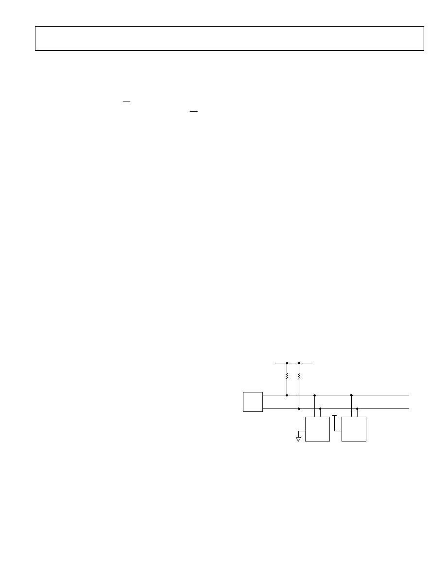
Multiple Devices on One Bus
Figure 44 shows two AD5161 devices on the same serial bus.
Each has a different slave address since the states of their AD0
pins are different. This allows each RDAC within each device to
be written to or read from independently. The master device
output bus line drivers are open-drain pull-downs in a fully I2C
compatible interface.
MASTER
AD5161
SDA SCL
RP
+5V
SDA
SCL
SDA SCL
AD5161
AD0
Figure 44. Multiple AD5161 Devices on One I2C Bus
相关PDF资料 |
PDF描述 |
|---|---|
| MS27474T22A35PA | CONN RCPT 100POS JAM NUT W/PINS |
| DS14285QN+ | IC RTC W/NV RAM CNTRL 28-PLCC |
| AD5110BCPZ80-1-RL7 | IC DGTL POT 128POS 80K 8LFCSP |
| M83723/76R16248 | CONN PLUG 24POS STRAIGHT W/PINS |
| DS14285N+ | IC RTC W/NV RAM CNTRL 24-DIP |
相关代理商/技术参数 |
参数描述 |
|---|---|
| AD5161BRM5 | 功能描述:IC POT DGTL 5K 256POS 10-MSOP RoHS:否 类别:集成电路 (IC) >> 数据采集 - 数字电位器 系列:- 标准包装:3,000 系列:DPP 接片:32 电阻(欧姆):10k 电路数:1 温度系数:标准值 300 ppm/°C 存储器类型:非易失 接口:3 线串行(芯片选择,递增,增/减) 电源电压:2.5 V ~ 6 V 工作温度:-40°C ~ 85°C 安装类型:表面贴装 封装/外壳:8-WFDFN 裸露焊盘 供应商设备封装:8-TDFN(2x3) 包装:带卷 (TR) |
| AD5161BRM50 | 功能描述:IC POT DGTL 50K 256POS 10-MSOP RoHS:否 类别:集成电路 (IC) >> 数据采集 - 数字电位器 系列:- 标准包装:3,000 系列:DPP 接片:32 电阻(欧姆):10k 电路数:1 温度系数:标准值 300 ppm/°C 存储器类型:非易失 接口:3 线串行(芯片选择,递增,增/减) 电源电压:2.5 V ~ 6 V 工作温度:-40°C ~ 85°C 安装类型:表面贴装 封装/外壳:8-WFDFN 裸露焊盘 供应商设备封装:8-TDFN(2x3) 包装:带卷 (TR) |
| AD5161BRM50-RL7 | 功能描述:IC DGTL POT SPI 256POS 10-MSOP RoHS:否 类别:集成电路 (IC) >> 数据采集 - 数字电位器 系列:- 标准包装:3,000 系列:DPP 接片:32 电阻(欧姆):10k 电路数:1 温度系数:标准值 300 ppm/°C 存储器类型:非易失 接口:3 线串行(芯片选择,递增,增/减) 电源电压:2.5 V ~ 6 V 工作温度:-40°C ~ 85°C 安装类型:表面贴装 封装/外壳:8-WFDFN 裸露焊盘 供应商设备封装:8-TDFN(2x3) 包装:带卷 (TR) |
| AD5161BRM5-RL7 | 功能描述:IC DGTL POT SPI 256POS 10-MSOP RoHS:否 类别:集成电路 (IC) >> 数据采集 - 数字电位器 系列:- 标准包装:3,000 系列:DPP 接片:32 电阻(欧姆):10k 电路数:1 温度系数:标准值 300 ppm/°C 存储器类型:非易失 接口:3 线串行(芯片选择,递增,增/减) 电源电压:2.5 V ~ 6 V 工作温度:-40°C ~ 85°C 安装类型:表面贴装 封装/外壳:8-WFDFN 裸露焊盘 供应商设备封装:8-TDFN(2x3) 包装:带卷 (TR) |
| AD5161BRMZ10 | 功能描述:IC DGTL POT SPI 10K 10-MSOP RoHS:是 类别:集成电路 (IC) >> 数据采集 - 数字电位器 系列:- 产品培训模块:Lead (SnPb) Finish for COTS Obsolescence Mitigation Program 标准包装:1 系列:- 接片:256 电阻(欧姆):100k 电路数:1 温度系数:标准值 35 ppm/°C 存储器类型:非易失 接口:3 线串口 电源电压:2.7 V ~ 5.25 V 工作温度:-40°C ~ 85°C 安装类型:表面贴装 封装/外壳:8-WDFN 裸露焊盘 供应商设备封装:8-TDFN-EP(3x3) 包装:剪切带 (CT) 产品目录页面:1399 (CN2011-ZH PDF) 其它名称:MAX5423ETA+TCT |
发布紧急采购,3分钟左右您将得到回复。