- 您现在的位置:买卖IC网 > PDF目录9298 > AD5204BRUZ50-REEL7 (Analog Devices Inc)IC POT DGTL QUAD 256POS 24TSSOP PDF资料下载
参数资料
| 型号: | AD5204BRUZ50-REEL7 |
| 厂商: | Analog Devices Inc |
| 文件页数: | 5/20页 |
| 文件大小: | 0K |
| 描述: | IC POT DGTL QUAD 256POS 24TSSOP |
| 标准包装: | 1,000 |
| 接片: | 256 |
| 电阻(欧姆): | 50k |
| 电路数: | 4 |
| 温度系数: | 标准值 700 ppm/°C |
| 存储器类型: | 易失 |
| 接口: | 4 线 SPI(芯片选择) |
| 电源电压: | 2.7 V ~ 5.5 V,±2.3 V ~ 2.7 V |
| 工作温度: | -40°C ~ 85°C |
| 安装类型: | 表面贴装 |
| 封装/外壳: | 24-TSSOP(0.173",4.40mm 宽) |
| 供应商设备封装: | 24-TSSOP |
| 包装: | 带卷 (TR) |
AD5204/AD5206
Rev. C | Page 13 of 20
PROGRAMMING THE VARIABLE RESISTOR
RHEOSTAT OPERATION
The nominal resistance of the RDAC between Terminal A and
Terminal B is available with values of 10 kΩ, 50 kΩ, and 100 kΩ.
The last digits of the part number determine the nominal
resistance value; for example, 10 kΩ = 10 and 100 kΩ = 100.
The nominal resistance (RAB) of the VR has 256 contact points
accessed by the wiper terminal, plus Terminal B contact. The
8-bit data-word in the RDAC latch is decoded to select one of
the 256 possible settings. The first connection of the wiper starts
at Terminal B for the 0x00 data. This Terminal B connection has a
wiper contact resistance of 45 Ω. The second connection (for a
10 kΩ part) is the first tap point, located at 84 Ω [= RAB (nominal
resistance)/256 + RW = 84 Ω + 45 Ω] for the 0x01 data. The
third connection is the next tap point, representing 78 + 45 =
123 Ω for the 0x02 data. Each LSB data value increase moves
the wiper up the resistor ladder until the last tap point is
reached at 10,006 Ω. The wiper does not directly connect to
Terminal A. See Figure 21 for a simplified diagram of the
equivalent RDAC circuit.
The general transfer equation determining the digitally
programmed output resistance between the Wx and Bx
terminals is
RWB (Dx) = (Dx)/256 × RAB + RW
(1)
where Dx is the data contained in the 8-bit RDACx latch, and
RAB is the nominal end-to-end resistance.
For example, when VB = 0 V and Terminal A is open circuited, the
output resistance values are set as outlined in Table 7 for the
RDAC latch codes (applies to the 10 kΩ potentiometer).
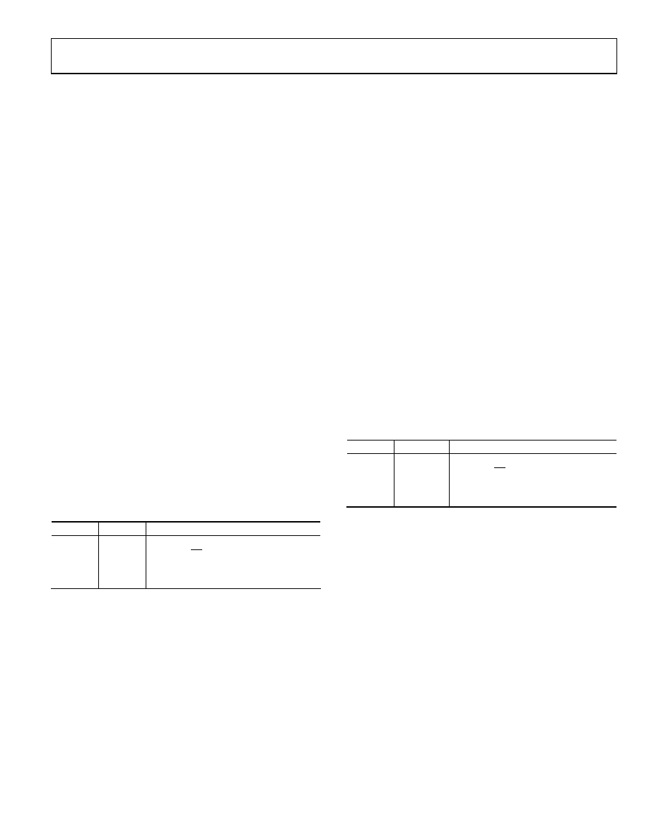
Table 7. Output Resistance Values for the RDAC Latch Codes—
VB = 0 V and Terminal A = Open Circuited
D (Dec)
RWB (Ω)
Output State
255
10006
Full scale
128
5045
Midscale (PR = 0 condition)
1
84
1 LSB
0
45
Zero scale (wiper contact resistance)
In the zero-scale condition, a finite total wiper resistance of 45 Ω
is present. Regardless of which setting the part is operating in,
care should be taken to limit the current between Terminal A to
Terminal B, Wiper W to Terminal A, and Wiper W to Terminal
B, to the maximum continuous current of ±5.65 mA(10 kΩ) or
±1.35 mA(50 kΩ and 100 kΩ) or pulse current of ±20 mA.
Otherwise, degradation or possible destruction of the internal
switch contact, can occur.
Like the mechanical potentiometer that the RDAC replaces,
the RDAC is completely symmetrical. The resistance between
Wiper W and Terminal A produces a digitally controlled
resistance, RWA. When these terminals are used, Terminal B
should be tied to the wiper. Setting the resistance value for RWA
starts at a maximum value of resistance and decreases as the
data loaded to the latch is increased in value. The general
transfer equation for this operation is
RWA (Dx) = (256 Dx)/256 × RAB + RW
(2)
where Dx is the data contained in the 8-bit RDACx latch, and
RAB is the nominal end-to-end resistance.
For example, when VA = 0 V and Terminal B is tied to Wiper W,
the output resistance values outlined in Table 8 are set for the
RDAC latch codes.
Table 8. Output Resistance Values for the RDAC Latch Codes—
VA = 0 V and Terminal B Tied to Wiper W
D (DEC)
RWA (Ω)
Output State
255
84
Full scale
128
5045
Midscale (PR = 0 condition)
1
10006
1 LSB
0
10045
Zero scale
The typical distribution of RAB from channel to channel matches
to within ±1%. However, device-to-device matching is process
lot dependent, having a ±30% variation. The change in RAB in
terms of temperature has a 700 ppm/°C temperature coefficient.
相关PDF资料 |
PDF描述 |
|---|---|
| VE-BND-MY-F1 | CONVERTER MOD DC/DC 85V 50W |
| VE-BNB-MY-F3 | CONVERTER MOD DC/DC 95V 50W |
| AD5204BRUZ100-R7 | IC POT DGTL QUAD 256POS 24TSSOP |
| VE-BNB-MY-F2 | CONVERTER MOD DC/DC 95V 50W |
| AD5204BRUZ10-REEL7 | IC POT DGTL QUAD 256POS 24TSSOP |
相关代理商/技术参数 |
参数描述 |
|---|---|
| AD5204BRZ10 | 功能描述:IC DGTL POT QUAD 10K 24-SOIC RoHS:是 类别:集成电路 (IC) >> 数据采集 - 数字电位器 系列:- 产品培训模块:Lead (SnPb) Finish for COTS Obsolescence Mitigation Program 标准包装:1 系列:- 接片:256 电阻(欧姆):100k 电路数:1 温度系数:标准值 35 ppm/°C 存储器类型:非易失 接口:3 线串口 电源电压:2.7 V ~ 5.25 V 工作温度:-40°C ~ 85°C 安装类型:表面贴装 封装/外壳:8-WDFN 裸露焊盘 供应商设备封装:8-TDFN-EP(3x3) 包装:剪切带 (CT) 产品目录页面:1399 (CN2011-ZH PDF) 其它名称:MAX5423ETA+TCT |
| AD5204BRZ100 | 功能描述:IC DGTL POT QUAD 100K 24-SOIC RoHS:是 类别:集成电路 (IC) >> 数据采集 - 数字电位器 系列:- 标准包装:3,000 系列:DPP 接片:32 电阻(欧姆):10k 电路数:1 温度系数:标准值 300 ppm/°C 存储器类型:非易失 接口:3 线串行(芯片选择,递增,增/减) 电源电压:2.5 V ~ 6 V 工作温度:-40°C ~ 85°C 安装类型:表面贴装 封装/外壳:8-WFDFN 裸露焊盘 供应商设备封装:8-TDFN(2x3) 包装:带卷 (TR) |
| AD5204BRZ100-REEL | 功能描述:IC DGTL POT QUAD 100K 24-SOIC RoHS:是 类别:集成电路 (IC) >> 数据采集 - 数字电位器 系列:- 标准包装:2,500 系列:XDCP™ 接片:256 电阻(欧姆):100k 电路数:1 温度系数:标准值 ±300 ppm/°C 存储器类型:非易失 接口:I²C(设备位址) 电源电压:2.7 V ~ 5.5 V 工作温度:0°C ~ 70°C 安装类型:表面贴装 封装/外壳:14-TSSOP(0.173",4.40mm 宽) 供应商设备封装:14-TSSOP 包装:带卷 (TR) |
| AD5204BRZ10-REEL | 功能描述:IC DGTL POT QUAD 10K 24-SOIC RoHS:是 类别:集成电路 (IC) >> 数据采集 - 数字电位器 系列:- 标准包装:3,000 系列:DPP 接片:32 电阻(欧姆):10k 电路数:1 温度系数:标准值 300 ppm/°C 存储器类型:非易失 接口:3 线串行(芯片选择,递增,增/减) 电源电压:2.5 V ~ 6 V 工作温度:-40°C ~ 85°C 安装类型:表面贴装 封装/外壳:8-WFDFN 裸露焊盘 供应商设备封装:8-TDFN(2x3) 包装:带卷 (TR) |
| AD5204BRZ50 | 功能描述:IC DGTL POT QUAD 50K 24-SOIC RoHS:是 类别:集成电路 (IC) >> 数据采集 - 数字电位器 系列:- 标准包装:2,500 系列:XDCP™ 接片:256 电阻(欧姆):100k 电路数:1 温度系数:标准值 ±300 ppm/°C 存储器类型:非易失 接口:I²C(设备位址) 电源电压:2.7 V ~ 5.5 V 工作温度:0°C ~ 70°C 安装类型:表面贴装 封装/外壳:14-TSSOP(0.173",4.40mm 宽) 供应商设备封装:14-TSSOP 包装:带卷 (TR) |
发布紧急采购,3分钟左右您将得到回复。