- 您现在的位置:买卖IC网 > PDF目录9298 > AD5204BRUZ50-REEL7 (Analog Devices Inc)IC POT DGTL QUAD 256POS 24TSSOP PDF资料下载
参数资料
| 型号: | AD5204BRUZ50-REEL7 |
| 厂商: | Analog Devices Inc |
| 文件页数: | 7/20页 |
| 文件大小: | 0K |
| 描述: | IC POT DGTL QUAD 256POS 24TSSOP |
| 标准包装: | 1,000 |
| 接片: | 256 |
| 电阻(欧姆): | 50k |
| 电路数: | 4 |
| 温度系数: | 标准值 700 ppm/°C |
| 存储器类型: | 易失 |
| 接口: | 4 线 SPI(芯片选择) |
| 电源电压: | 2.7 V ~ 5.5 V,±2.3 V ~ 2.7 V |
| 工作温度: | -40°C ~ 85°C |
| 安装类型: | 表面贴装 |
| 封装/外壳: | 24-TSSOP(0.173",4.40mm 宽) |
| 供应商设备封装: | 24-TSSOP |
| 包装: | 带卷 (TR) |
AD5204/AD5206
Rev. C | Page 15 of 20
DIGITAL INTERFACING
The AD5204/AD5206 each contain a standard 3-wire serial
input control interface. The three inputs are clock (CLK), chip
select input (CS), and serial data input (SDI). The positive-
edge-sensitive CLK input requires clean transitions to avoid
clocking incorrect data into the serial input register. Standard
logic families work well. If mechanical switches are used for
product evaluation, they should be debounced by a flip-flop or
by other suitable means.
shows more detail of the
internal digital circuitry. When
CS is taken active low, the clock
loads data into the serial register on each positive clock edge
(see
). When using a positive (VDD) and negative (VSS)
supply voltage, the logic levels are still referenced to digital
ground (GND).
The serial data output (SDO) pin contains an open-drain
n-channel FET. This output requires a pull-up resistor to transfer
data to the SDI pin of the next package. The pull-up resistor
termination voltage can be larger than the VDD supply of the
AD5204. For example, the AD5204 can operate at VDD = 3.3 V,
and the pull-up for the interface to the next device can be set at
5 V. This allows for daisy chaining several RDACs from a
single-processor serial data line.
If a pull-up resistor is used to connect the SDI pin of the
next device in the series, the clock period must be increased.
Capacitive loading at the daisy-chain node (where SDO and
SDI are connected) between the devices must be accounted for
to successfully transfer data. When daisy chaining is used, the
CS should be kept low until all the bits of every package are
clocked into their respective serial registers, ensuring that the
address bits and data bits are in the proper decoding locations.
This requires 22 bits of address and data complying to the data-
word format outlined in
if two AD5204 4-channel RDACs
are daisy-chained. During shutdown (
SHDN), the SDO output
pin is forced to the off (logic high state) position to disable power
dissipation in the pull-up resistor. See
for the equivalent
SDO output circuit schematic.
Table 9. Input Logic Control Truth Table1
CLK
CS
PR
SHDN
Register Activity
L
H
No SR effect; enables SDO pin.
P
L
H
Shift one bit in from the SDI pin. The
11th bit entered is shifted out of the
SDO pin.
X
P
H
Load SR data into the RDAC latch
based on A2, A1, A0 decode (Table 10).
X
H
No operation.
X
L
H
Sets all RDAC latches to midscale;
wiper centered and SDO latch
cleared.
X
H
P
H
Latches all RDAC latches to 0x80.
X
H
L
Open circuits all A resistor terminals,
connects Wiper W to Terminal B, and
turns off the SDO output transistor.
1 P = positive edge, X = don’t care, SR = shift register.
Table 10. Address Decode Table
A2
A1
A0
Latch Decoded
0
RDAC 1
0
1
RDAC 2
0
1
0
RDAC 3
0
1
RDAC 4
1
0
RDAC 5 AD5206 only
1
0
1
RDAC 6 AD5206 only
The data setup and data hold times in the specification table
determine the data valid time requirements. The last 11 bits of
the data-word entered into the serial register are held when CS
returns high. When CS goes high, the address decoder is gated,
enabling one of four or six positive-edge-triggered RDAC
latches (see
for details).
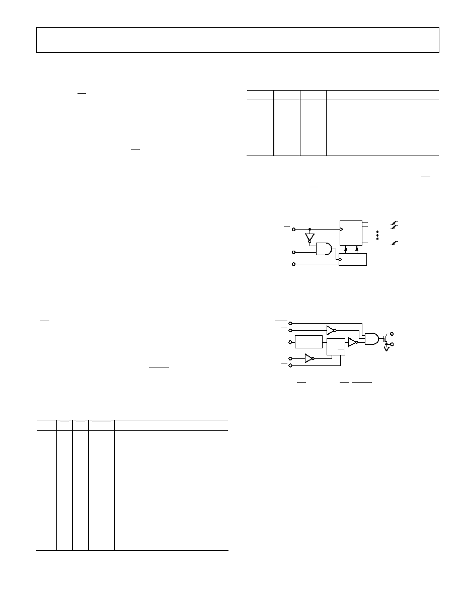
ADDR
DECODE
RDAC 1
RDAC 2
RDAC 4/
RDAC 6
SERIAL
REGISTER
AD5204/AD5206
SDI
CLK
CS
06
88
4-
04
8
Figure 23. Equivalent Input Control Logic
The target RDAC latch is loaded with the last eight bits of the
serial data-word, completing one DAC update. Four separate
8-bit data-words must be clocked in to change all four VR
settings.
SERIAL
REGISTER
SDI
CK RS
D
SHDN
CS
CLK
PR
SDO
GND
Q
06
88
4-
0
49
Figure 24. Detail SDO Output Schematic of the AD5204
All digital pins (CS, SDI, SDO, PR, SHDN, and CLK) are
protected with a series input resistor and a parallel Zener ESD
structure (see
).
相关PDF资料 |
PDF描述 |
|---|---|
| VE-BND-MY-F1 | CONVERTER MOD DC/DC 85V 50W |
| VE-BNB-MY-F3 | CONVERTER MOD DC/DC 95V 50W |
| AD5204BRUZ100-R7 | IC POT DGTL QUAD 256POS 24TSSOP |
| VE-BNB-MY-F2 | CONVERTER MOD DC/DC 95V 50W |
| AD5204BRUZ10-REEL7 | IC POT DGTL QUAD 256POS 24TSSOP |
相关代理商/技术参数 |
参数描述 |
|---|---|
| AD5204BRZ10 | 功能描述:IC DGTL POT QUAD 10K 24-SOIC RoHS:是 类别:集成电路 (IC) >> 数据采集 - 数字电位器 系列:- 产品培训模块:Lead (SnPb) Finish for COTS Obsolescence Mitigation Program 标准包装:1 系列:- 接片:256 电阻(欧姆):100k 电路数:1 温度系数:标准值 35 ppm/°C 存储器类型:非易失 接口:3 线串口 电源电压:2.7 V ~ 5.25 V 工作温度:-40°C ~ 85°C 安装类型:表面贴装 封装/外壳:8-WDFN 裸露焊盘 供应商设备封装:8-TDFN-EP(3x3) 包装:剪切带 (CT) 产品目录页面:1399 (CN2011-ZH PDF) 其它名称:MAX5423ETA+TCT |
| AD5204BRZ100 | 功能描述:IC DGTL POT QUAD 100K 24-SOIC RoHS:是 类别:集成电路 (IC) >> 数据采集 - 数字电位器 系列:- 标准包装:3,000 系列:DPP 接片:32 电阻(欧姆):10k 电路数:1 温度系数:标准值 300 ppm/°C 存储器类型:非易失 接口:3 线串行(芯片选择,递增,增/减) 电源电压:2.5 V ~ 6 V 工作温度:-40°C ~ 85°C 安装类型:表面贴装 封装/外壳:8-WFDFN 裸露焊盘 供应商设备封装:8-TDFN(2x3) 包装:带卷 (TR) |
| AD5204BRZ100-REEL | 功能描述:IC DGTL POT QUAD 100K 24-SOIC RoHS:是 类别:集成电路 (IC) >> 数据采集 - 数字电位器 系列:- 标准包装:2,500 系列:XDCP™ 接片:256 电阻(欧姆):100k 电路数:1 温度系数:标准值 ±300 ppm/°C 存储器类型:非易失 接口:I²C(设备位址) 电源电压:2.7 V ~ 5.5 V 工作温度:0°C ~ 70°C 安装类型:表面贴装 封装/外壳:14-TSSOP(0.173",4.40mm 宽) 供应商设备封装:14-TSSOP 包装:带卷 (TR) |
| AD5204BRZ10-REEL | 功能描述:IC DGTL POT QUAD 10K 24-SOIC RoHS:是 类别:集成电路 (IC) >> 数据采集 - 数字电位器 系列:- 标准包装:3,000 系列:DPP 接片:32 电阻(欧姆):10k 电路数:1 温度系数:标准值 300 ppm/°C 存储器类型:非易失 接口:3 线串行(芯片选择,递增,增/减) 电源电压:2.5 V ~ 6 V 工作温度:-40°C ~ 85°C 安装类型:表面贴装 封装/外壳:8-WFDFN 裸露焊盘 供应商设备封装:8-TDFN(2x3) 包装:带卷 (TR) |
| AD5204BRZ50 | 功能描述:IC DGTL POT QUAD 50K 24-SOIC RoHS:是 类别:集成电路 (IC) >> 数据采集 - 数字电位器 系列:- 标准包装:2,500 系列:XDCP™ 接片:256 电阻(欧姆):100k 电路数:1 温度系数:标准值 ±300 ppm/°C 存储器类型:非易失 接口:I²C(设备位址) 电源电压:2.7 V ~ 5.5 V 工作温度:0°C ~ 70°C 安装类型:表面贴装 封装/外壳:14-TSSOP(0.173",4.40mm 宽) 供应商设备封装:14-TSSOP 包装:带卷 (TR) |
发布紧急采购,3分钟左右您将得到回复。