- 您现在的位置:买卖IC网 > PDF目录9281 > AD5235BRUZ250-R7 (Analog Devices Inc)IC DGTL POT DUAL 1024POS 16TSSOP PDF资料下载
参数资料
| 型号: | AD5235BRUZ250-R7 |
| 厂商: | Analog Devices Inc |
| 文件页数: | 10/32页 |
| 文件大小: | 0K |
| 描述: | IC DGTL POT DUAL 1024POS 16TSSOP |
| 产品变化通告: | Metal Edit Change 03/Feb/2012 |
| 标准包装: | 1,000 |
| 接片: | 1024 |
| 电阻(欧姆): | 250k |
| 电路数: | 2 |
| 温度系数: | 标准值 35 ppm/°C |
| 存储器类型: | 非易失 |
| 接口: | 4 线 SPI(芯片选择) |
| 电源电压: | 3 V ~ 5.5 V,±2.25 V ~ 2.75 V |
| 工作温度: | -40°C ~ 85°C |
| 安装类型: | 表面贴装 |
| 封装/外壳: | 16-TSSOP(0.173",4.40mm 宽) |
| 供应商设备封装: | 16-TSSOP |
| 包装: | 带卷 (TR) |
第1页第2页第3页第4页第5页第6页第7页第8页第9页当前第10页第11页第12页第13页第14页第15页第16页第17页第18页第19页第20页第21页第22页第23页第24页第25页第26页第27页第28页第29页第30页第31页第32页
AD5235
Data Sheet
Rev. F | Page 18 of 32
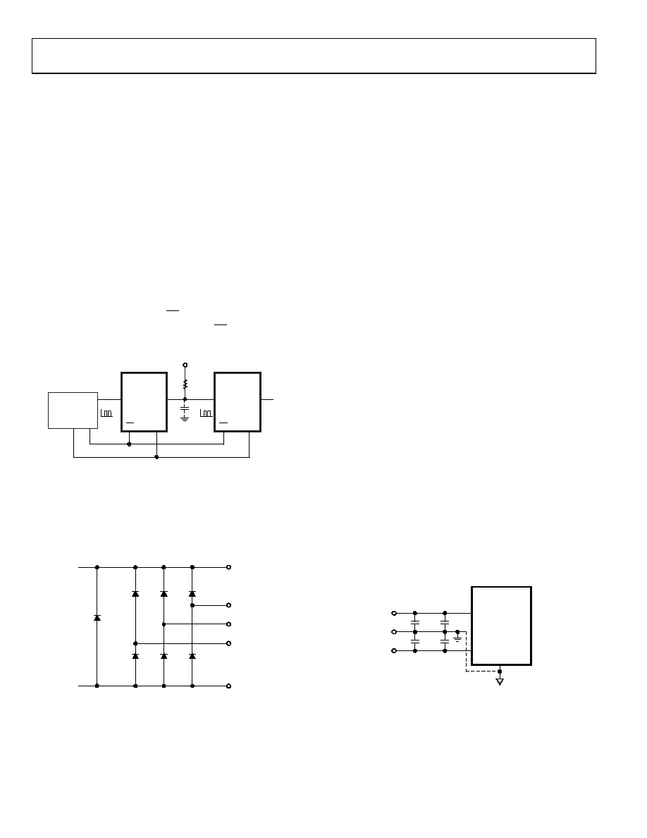
DAISY-CHAIN OPERATION
The serial data output pin (SDO) serves two purposes. It can be
used to read the contents of the wiper setting and EEMEM values
using Instruction 10 and Instruction 9, respectively. The remaining
instructions (Instruction 0 to Instruction 8, Instruction 11 to
Instruction 15) are valid for daisy-chaining multiple devices in
simultaneous operations. Daisy-chaining minimizes the number
of port pins required from the controlling IC (see Figure 41). The
SDO pin contains an open-drain N-Ch FET that requires a pull-up
resistor, if this function is used. As shown in Figure 41, users need
to tie the SDO pin of one package to the SDI pin of the next package.
Users may need to increase the clock period because the pull-up
resistor and the capacitive loading at the SDO-to-SDI interface may
require additional time delay between subsequent devices.
When two AD5235s are daisy-chained, 48 bits of data are
required. The first 24 bits (formatted 4-bit command, 4-bit
address, and 16-bit data) go to U2, and the second 24 bits with
the same format go to U1. Keep CS low until all 48 bits are
clocked into their respective serial registers. CS is then pulled
high to complete the operation.
CLK
RP
2.2k
SDI
SDO
U2
AD5235
CS
CLK
SDI
SDO
U1
AD5235
CS
VDD
SCLK SS
MOSI
MICRO-
CONTROLLER
02
81
6-
0
40
Figure 41. Daisy-Chain Configuration Using SDO
TERMINAL VOLTAGE OPERATING RANGE
The positive VDD and negative VSS power supplies of the AD5235
define the boundary conditions for proper 3-terminal digital
potentiometer operation. Supply signals present on Terminal A,
Terminal B, and Terminal W that exceed VDD or VSS are clamped by
the internal forward-biased diodes (see Figure 42).
VSS
VDD
A
W
B
02
81
6-
04
1
Figure 42. Maximum Terminal Voltages Set by VDD and VSS
The GND pin of the AD5235 is primarily used as a digital
ground reference. To minimize the digital ground bounce,
the AD5235 ground terminal should be joined remotely to
the common ground (see Figure 43). The digital input control
signals to the AD5235 must be referenced to the device ground
pin (GND) and must satisfy the logic level defined in the
Specifications section. An internal level-shift circuit ensures
that the common-mode voltage range of the three terminals
extends from VSS to VDD, regardless of the digital input level.
Power-Up Sequence
Because there are diodes to limit the voltage compliance at
Terminal A, Terminal B, and Terminal W (see Figure 42), it
is important to power VDD and VSS first before applying any
voltage to Terminal A, Terminal B, and Terminal W. Otherwise,
the diode is forward-biased such that VDD and VSS are powered
unintentionally. For example, applying 5 V across Terminal A
and Terminal B prior to VDD causes the VDD terminal to exhibit
4.3 V. It is not destructive to the device, but it might affect the
rest of the user’s system. The ideal power-up sequence is GND,
VDD and VSS, digital inputs, and VA, VB, and VW. The order of
powering VA, VB, VW, and the digital inputs is not important as
long as they are powered after VDD and VSS.
Regardless of the power-up sequence and the ramp rates of the
power supplies, when VDD and VSS are powered, the power-on
preset activates, which restores the EEMEM values to the RDAC
registers.
Layout and Power Supply Bypassing
It is a good practice to employ compact, minimum lead-length
layout design. The leads to the input should be as direct as
possible with a minimum conductor length. Ground paths
should have low resistance and low inductance.
Similarly, it is good practice to bypass the power supplies with
quality capacitors for optimum stability. Bypass supply leads to
the device with 0.01 μF to 0.1 μF disk or chip ceramic capacitors.
Also, apply low ESR, 1 μF to 10 μF tantalum or electrolytic
capacitors at the supplies to minimize any transient disturbance
(see Figure 43).
AD5235
VDD
GND
02
81
6-
04
2
VSS
C3
10F
C4
10F
C2
0.1F
C1
0.1F
+
VDD
VSS
Figure 43. Power Supply Bypassing
相关PDF资料 |
PDF描述 |
|---|---|
| DS1135Z-8+T&R | IC DELAY LINE 8NS 8-SOIC |
| AD5235BRUZ25-RL7 | IC DGTL POT DUAL 1024POS 16TSSOP |
| VI-2TP-MW | CONVERTER MOD DC/DC 13.8V 100W |
| DS1135Z-12+T&R | IC DELAY LINE 12NS 8-SOIC |
| DS1135Z-20+T&R | IC DELAY LINE 20NS 8-SOIC |
相关代理商/技术参数 |
参数描述 |
|---|---|
| AD5235BRUZ25-EP-R7 | 功能描述:IC DGTL POT 1024POS DUAL 16TSSOP 制造商:analog devices inc. 系列:* 零件状态:在售 标准包装:1,000 |
| AD5235BRUZ25-RL7 | 功能描述:IC DGTL POT DUAL 1024POS 16TSSOP RoHS:是 类别:集成电路 (IC) >> 数据采集 - 数字电位器 系列:- 标准包装:3,000 系列:DPP 接片:32 电阻(欧姆):10k 电路数:1 温度系数:标准值 300 ppm/°C 存储器类型:非易失 接口:3 线串行(芯片选择,递增,增/减) 电源电压:2.5 V ~ 6 V 工作温度:-40°C ~ 85°C 安装类型:表面贴装 封装/外壳:8-WFDFN 裸露焊盘 供应商设备封装:8-TDFN(2x3) 包装:带卷 (TR) |
| AD5235-EP | 制造商:AD 制造商全称:Analog Devices 功能描述:Nonvolatile Memory, Dual 1024-Position Digital Potentiometer |
| AD5235EVAL | 制造商:Analog Devices 功能描述:DUAL 10BIT SPI EVAL BOARD - Bulk |
| AD5235EVAL25 | 制造商:Analog Devices 功能描述:Evaluation Board For 1024-Position Digital Potentiometer 制造商:Analog Devices 功能描述:DUAL 10BIT SPI EVAL BOARD - Bulk |
发布紧急采购,3分钟左右您将得到回复。