- 您现在的位置:买卖IC网 > PDF目录9163 > AD5242BRU10-REEL7 (Analog Devices Inc)IC DGTL POT 256POS 16-TSSOP T/R PDF资料下载
参数资料
| 型号: | AD5242BRU10-REEL7 |
| 厂商: | Analog Devices Inc |
| 文件页数: | 4/20页 |
| 文件大小: | 0K |
| 描述: | IC DGTL POT 256POS 16-TSSOP T/R |
| 产品变化通告: | Product Discontinuance 27/Oct/2011 |
| 标准包装: | 1,000 |
| 接片: | 256 |
| 电阻(欧姆): | 10k |
| 电路数: | 2 |
| 温度系数: | 标准值 30 ppm/°C |
| 存储器类型: | 易失 |
| 接口: | I²C(设备位址) |
| 电源电压: | 2.7 V ~ 5.5 V,±2.3 V ~ 2.7 V |
| 工作温度: | -40°C ~ 105°C |
| 安装类型: | 表面贴装 |
| 封装/外壳: | 16-TSSOP(0.173",4.40mm 宽) |
| 供应商设备封装: | 16-TSSOP |
| 包装: | 带卷 (TR) |
| 配用: | EVAL-AD5242EBZ-ND - BOARD EVALUATION FOR AD5242 |
AD5241/AD5242
Rev. C | Page 12 of 20
THEORY OF OPERATION
The AD5241/AD5242 provide a single-/dual-channel, 256-
position digitally controlled variable resistor (VR) device. The
terms VR, RDAC, and programmable resistor are commonly
used interchangeably to refer to digital potentiometer.
To program the VR settings, refer to the Digital Interface section.
Both parts have an internal power-on preset that places the wiper
in midscale during power-on that simplifies the fault condition
recovery at power-up. In addition, the shutdown pin (SHDN)
of AD5241/AD5242 places the RDAC in an almost zero power
consumption state where Terminal A is open circuited and Wiper
W is connected to Terminal B, resulting in only leakage current
being consumed in the VR structure. During shutdown, the VR
latch contents are maintained when the RDAC is inactive. When
the part returns from shutdown, the stored VR setting is applied
to the RDAC.
SWSHDN
SW N
2–1
R
SW N
2–2
RDAC
LATCH
AND
DECODER
RRAB/2N
B
W
DIGITAL CIRCUITRY
OMITTED FOR CLARITY
A
SW1
SW0
R
D7
D6
D5
D4
D3
D2
D1
D0
SHDN
00
92
6-
02
2
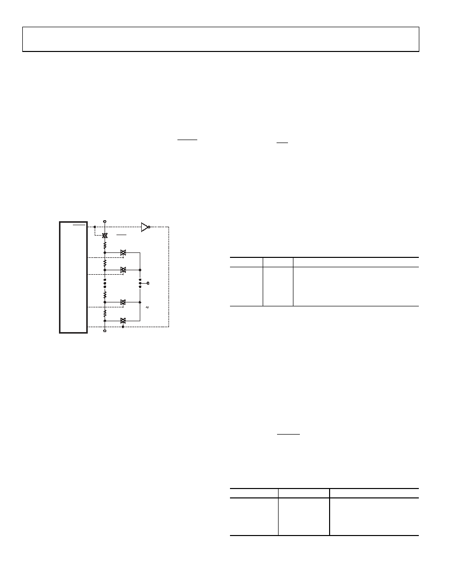
Figure 31. Equivalent RDAC Circuit
PROGRAMMING THE VARIABLE RESISTOR
Rheostat Operation
The nominal resistance of the RDAC between Terminal A and
Terminal B is available in 10 kΩ, 100 kΩ, and 1 MΩ. The final two
or three digits of the part number determine the nominal resistance
value, for example, 10 kΩ = 10, 100 kΩ = 100, and 1 MΩ = 1 M.
The nominal resistance (RAB) of the VR has 256 contact points
accessed by the wiper terminal, plus the B terminal contact. The
8-bit data in the RDAC latch is decoded to select one of the 256
possible settings. Assume a 10 kΩ part is used; the first connection
of the wiper starts at the B terminal for Data 0x00. Because there is
a 60 Ω wiper contact resistance, such connection yields a minimum
of 60 Ω resistance between Terminal W and Terminal B. The
second connection is the first tap point that corresponds to 99 Ω
(RWB = RAB/256 + RW = 39 + 60) for Data 0x01. The third connection
is the next tap point representing 138 Ω (39 × 2 + 60) for Data 0x02,
and so on. Each LSB data value increase moves the wiper up the
resistor ladder until the last tap point is reached at 10,021 Ω
[RAB – 1 LSB + RW].
Figure 31 shows a simplified diagram of the equivalent RDAC
circuit where the last resistor string is not accessed; therefore,
there is 1 LSB less of the nominal resistance at full scale in
addition to the wiper resistance.
The general equation determining the digitally programmed
resistance between W and B is
RWB(D) =
256
D
× RAB + RW
(1)
where:
D is the decimal equivalent of the binary code between 0 and 255,
which is loaded in the 8-bit RDAC register.
RAB is the nominal end-to-end resistance.
RW is the wiper resistance contributed by the on resistance of
the internal switch.
Again, if RAB = 10 kΩ, Terminal A can be either open circuit or
set in the RDAC latch.
Table 6. RWB (D) at Selected Codes for RAB = 10 kΩ
D (DEC)
RWB (Ω)
Output State
255
10021
Full-scale (RWB – 1 LSB + RW)
128
5060
Midscale
1
99
1 LSB
0
60
Zero-scale (wiper contact resistance)
Note that in the zero-scale condition, a finite wiper resistance of
60 Ω is present. Care should be taken to limit the current flow
between W and B in this state to a maximum current of no more
than 20 mA. Otherwise, degradation or possible destruction of
the internal switch contact can occur.
Similar to the mechanical potentiometer, the resistance of the
RDAC between Wiper W and Terminal A also produces a
digitally controlled resistance, RWA. When these terminals are
used, Terminal B can be opened or tied to the wiper terminal.
The minimum RWA resistance is for Data 0xFF and increases as
the data loaded in the latch decreases in value. The general
equation for this operation is
RWA(D) =
256
256 D
× RAB + RW
(2)
For RAB = 10 kΩ, Terminal B can be either open circuit or tied
the RDAC latch.
Table 7. RWA (D) at Selected Codes for RAB = 10 kΩ
D (DEC)
RWA (Ω)
Output State
255
99
Full-scale
128
5060
Midscale
1
10021
1 LSB
0
10060
Zero-scale
相关PDF资料 |
PDF描述 |
|---|---|
| M83723/74R2039N | CONN RCPT 39POS JAM NUT W/PINS |
| MS27474E16A55S | CONN RCPT 55POS JAM NUT W/SCKT |
| AD5242BRU10 | IC DGTL POT 256POS 16-TSSOP |
| MS3116P16-26S | CONN PLUG 26POS STRAIGHT W/SCKT |
| AD5242BR1M | IC DGTL POT 256POS 16-SOIC |
相关代理商/技术参数 |
参数描述 |
|---|---|
| AD5242BRU10Z | 制造商:Analog Devices 功能描述:DIG POT 256 5.5V 10KOHM 14 |
| AD5242BRU1M | 功能描述:IC DGTL POT 256POS 16-TSSOP RoHS:否 类别:集成电路 (IC) >> 数据采集 - 数字电位器 系列:- 标准包装:3,000 系列:DPP 接片:32 电阻(欧姆):10k 电路数:1 温度系数:标准值 300 ppm/°C 存储器类型:非易失 接口:3 线串行(芯片选择,递增,增/减) 电源电压:2.5 V ~ 6 V 工作温度:-40°C ~ 85°C 安装类型:表面贴装 封装/外壳:8-WFDFN 裸露焊盘 供应商设备封装:8-TDFN(2x3) 包装:带卷 (TR) |
| AD5242BRU1M-REEL7 | 功能描述:IC DGTL POT 256POS 16-TSSOP T/R RoHS:否 类别:集成电路 (IC) >> 数据采集 - 数字电位器 系列:- 标准包装:2,500 系列:XDCP™ 接片:256 电阻(欧姆):100k 电路数:1 温度系数:标准值 ±300 ppm/°C 存储器类型:非易失 接口:I²C(设备位址) 电源电压:2.7 V ~ 5.5 V 工作温度:0°C ~ 70°C 安装类型:表面贴装 封装/外壳:14-TSSOP(0.173",4.40mm 宽) 供应商设备封装:14-TSSOP 包装:带卷 (TR) |
| AD5242BRU-REEL7 | 制造商:Analog Devices 功能描述:I2C? COMPATIBLE DIGITAL POTENTIOMETER - Tape and Reel |
| AD5242BRUZ10 | 功能描述:IC DGTL POT 256POS 16-TSSOP RoHS:是 类别:集成电路 (IC) >> 数据采集 - 数字电位器 系列:- 产品培训模块:Lead (SnPb) Finish for COTS Obsolescence Mitigation Program 标准包装:1 系列:- 接片:256 电阻(欧姆):100k 电路数:1 温度系数:标准值 35 ppm/°C 存储器类型:非易失 接口:3 线串口 电源电压:2.7 V ~ 5.25 V 工作温度:-40°C ~ 85°C 安装类型:表面贴装 封装/外壳:8-WDFN 裸露焊盘 供应商设备封装:8-TDFN-EP(3x3) 包装:剪切带 (CT) 产品目录页面:1399 (CN2011-ZH PDF) 其它名称:MAX5423ETA+TCT |
发布紧急采购,3分钟左右您将得到回复。