- 您现在的位置:买卖IC网 > PDF目录9163 > AD5242BRU10-REEL7 (Analog Devices Inc)IC DGTL POT 256POS 16-TSSOP T/R PDF资料下载
参数资料
| 型号: | AD5242BRU10-REEL7 |
| 厂商: | Analog Devices Inc |
| 文件页数: | 6/20页 |
| 文件大小: | 0K |
| 描述: | IC DGTL POT 256POS 16-TSSOP T/R |
| 产品变化通告: | Product Discontinuance 27/Oct/2011 |
| 标准包装: | 1,000 |
| 接片: | 256 |
| 电阻(欧姆): | 10k |
| 电路数: | 2 |
| 温度系数: | 标准值 30 ppm/°C |
| 存储器类型: | 易失 |
| 接口: | I²C(设备位址) |
| 电源电压: | 2.7 V ~ 5.5 V,±2.3 V ~ 2.7 V |
| 工作温度: | -40°C ~ 105°C |
| 安装类型: | 表面贴装 |
| 封装/外壳: | 16-TSSOP(0.173",4.40mm 宽) |
| 供应商设备封装: | 16-TSSOP |
| 包装: | 带卷 (TR) |
| 配用: | EVAL-AD5242EBZ-ND - BOARD EVALUATION FOR AD5242 |
AD5241/AD5242
Rev. C | Page 14 of 20
4.
Unlike the write mode, the data byte follows immediately
after the acknowledgment of the slave address byte in
Frame 2 read mode. Data is transmitted over the serial bus
in sequences of nine clock pulses (slightly different from
the write mode, there are eight data bits followed by a no
acknowledge Logic 1 bit in read mode). Similarly, the
transitions on the SDA line must occur during the low
period of SCL and remain stable during the high period of
SCL (see Figure 5).
MULTIPLE DEVICES ON ONE BUS
Figure 33 shows four AD5242 devices on the same serial bus.
Each has a different slave address because the state of their AD0
and AD1 pins are different. This allows each RDAC within each
device to be written to or read from independently. The master
device output bus line drivers are open-drain pull-downs in a
fully I2C-compatible interface. Note, a device is addressed properly
only if the bit information of AD0 and AD1 in the slave address
byte matches with the logic inputs at the AD0 and AD1 pins of
that particular device.
5.
When all data bits have been read or written, a stop condition
is established by the master. A stop condition is defined as
a low-to-high transition on the SDA line while SCL is high.
In write mode, the master pulls the SDA line high during
the tenth clock pulse to establish a stop condition (see
Figure 4). In read mode, the master issues a no acknowledge
for the ninth clock pulse (that is, the SDA line remains high).
The master then brings the SDA line low before the tenth
clock pulse, which goes high to establish a stop condition
(see Figure 5).
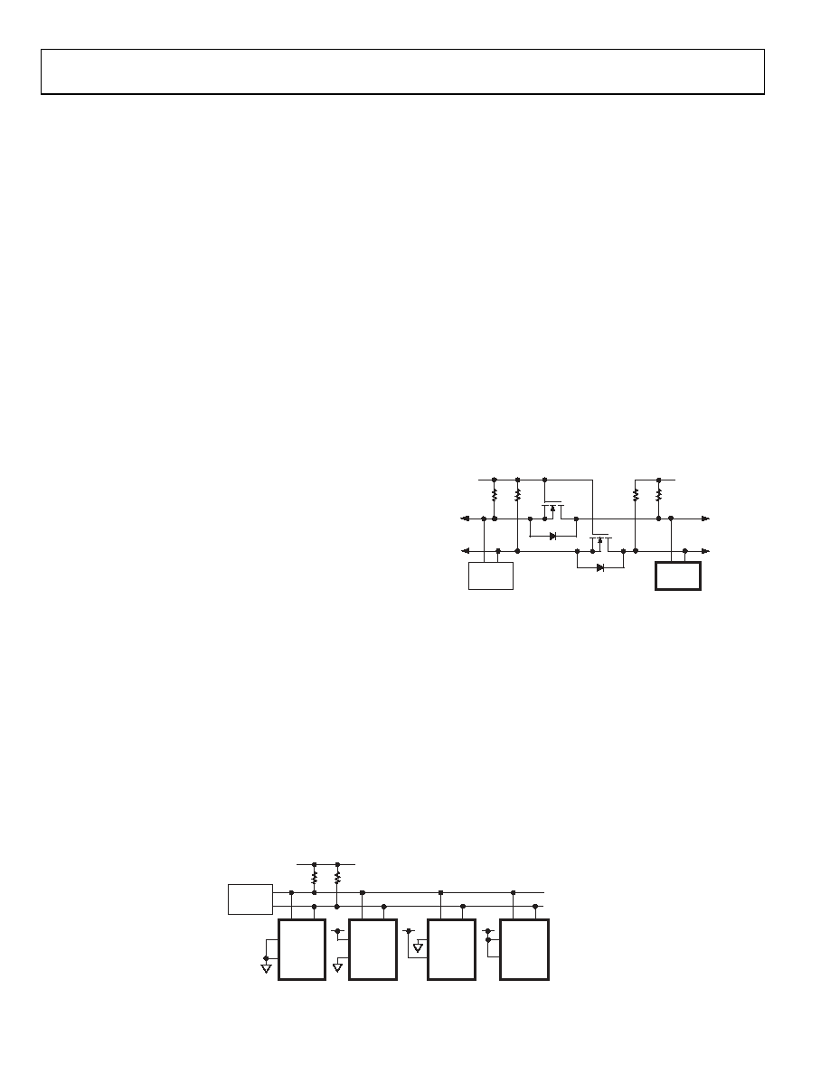
LEVEL-SHIFT FOR BIDIRECTIONAL INTERFACE
While most old systems can operate at one voltage, a new
component may be optimized at another. When they operate
the same signal at two different voltages, a proper method of
level-shifting is needed. For instance, a 3.3 V E2PROM can be
used to interface with a 5 V digital potentiometer. A level-shift
scheme is needed to enable a bidirectional communication so that
the setting of the digital potentiometer can be stored to and
M1 and M2 can be N-channel FETs (2N7002) or low threshold
FDV301N if VDD falls below 2.5 V.
A repeated write function gives the user flexibility to update the
RDAC output a number of times after addressing and instructing
the part only once. During the write cycle, each data byte updates
the RDAC output. For example, after the RDAC has acknowledged
its slave address and instruction bytes, the RDAC output is
updated. If another byte is written to the RDAC while it is still
addressed to a specific slave device with the same instruction,
this byte updates the output of the selected slave device. If
different instructions are needed, the write mode has to start a
completely new sequence with a new slave address, instruction,
and data bytes transferred again. Similarly, a repeated read
function of the RDAC is also allowed.
RP
SD
G
M1
G
M2
3.3V
E2PROM
RP
5V
AD5242
SCL2
SDA2
VDD = 5V
VDD = 3.3V
SCL1
SDA1
0
09
26
-02
4
Figure 32. Level-Shift for Different Voltage Devices Operation
READBACK RDAC VALUE
Specific to the AD5242 dual-channel device, the channel of
interest is the one that was previously selected in the write mode.
In addition, to read both RDAC values consecutively, users have to
perform two write-read cycles. For example, users may first specify
the RDAC1 subaddress in write mode (it is not necessary to issue
the data byte and stop condition), and then change to read mode
to read the RDAC1 value. To continue reading the RDAC2 value,
users have to switch back to write mode, specify the subaddress,
and then switch once again to read mode to read the RDAC2
value. It is not necessary to issue the write mode data byte or
the first stop condition for this operation. Users should refer to
SDA SCL
AD5242
AD1
AD0
SDA
SCL
RP
SDA SCL
AD5242
VDD
AD1
AD0
SDA SCL
AD1
AD0
AD5242
VDD
SDA SCL
AD5242
VDD
AD1
AD0
MASTER
5V
0
09
26
-02
3
Figure 33. Multiple AD5242 Devices on One Bus
相关PDF资料 |
PDF描述 |
|---|---|
| M83723/74R2039N | CONN RCPT 39POS JAM NUT W/PINS |
| MS27474E16A55S | CONN RCPT 55POS JAM NUT W/SCKT |
| AD5242BRU10 | IC DGTL POT 256POS 16-TSSOP |
| MS3116P16-26S | CONN PLUG 26POS STRAIGHT W/SCKT |
| AD5242BR1M | IC DGTL POT 256POS 16-SOIC |
相关代理商/技术参数 |
参数描述 |
|---|---|
| AD5242BRU10Z | 制造商:Analog Devices 功能描述:DIG POT 256 5.5V 10KOHM 14 |
| AD5242BRU1M | 功能描述:IC DGTL POT 256POS 16-TSSOP RoHS:否 类别:集成电路 (IC) >> 数据采集 - 数字电位器 系列:- 标准包装:3,000 系列:DPP 接片:32 电阻(欧姆):10k 电路数:1 温度系数:标准值 300 ppm/°C 存储器类型:非易失 接口:3 线串行(芯片选择,递增,增/减) 电源电压:2.5 V ~ 6 V 工作温度:-40°C ~ 85°C 安装类型:表面贴装 封装/外壳:8-WFDFN 裸露焊盘 供应商设备封装:8-TDFN(2x3) 包装:带卷 (TR) |
| AD5242BRU1M-REEL7 | 功能描述:IC DGTL POT 256POS 16-TSSOP T/R RoHS:否 类别:集成电路 (IC) >> 数据采集 - 数字电位器 系列:- 标准包装:2,500 系列:XDCP™ 接片:256 电阻(欧姆):100k 电路数:1 温度系数:标准值 ±300 ppm/°C 存储器类型:非易失 接口:I²C(设备位址) 电源电压:2.7 V ~ 5.5 V 工作温度:0°C ~ 70°C 安装类型:表面贴装 封装/外壳:14-TSSOP(0.173",4.40mm 宽) 供应商设备封装:14-TSSOP 包装:带卷 (TR) |
| AD5242BRU-REEL7 | 制造商:Analog Devices 功能描述:I2C? COMPATIBLE DIGITAL POTENTIOMETER - Tape and Reel |
| AD5242BRUZ10 | 功能描述:IC DGTL POT 256POS 16-TSSOP RoHS:是 类别:集成电路 (IC) >> 数据采集 - 数字电位器 系列:- 产品培训模块:Lead (SnPb) Finish for COTS Obsolescence Mitigation Program 标准包装:1 系列:- 接片:256 电阻(欧姆):100k 电路数:1 温度系数:标准值 35 ppm/°C 存储器类型:非易失 接口:3 线串口 电源电压:2.7 V ~ 5.25 V 工作温度:-40°C ~ 85°C 安装类型:表面贴装 封装/外壳:8-WDFN 裸露焊盘 供应商设备封装:8-TDFN-EP(3x3) 包装:剪切带 (CT) 产品目录页面:1399 (CN2011-ZH PDF) 其它名称:MAX5423ETA+TCT |
发布紧急采购,3分钟左右您将得到回复。