- 您现在的位置:买卖IC网 > PDF目录373873 > AD5245BRJ100-R2 (ANALOG DEVICES INC) CAP CERAMIC 10PF 50V NP0 0402 PDF资料下载
参数资料
| 型号: | AD5245BRJ100-R2 |
| 厂商: | ANALOG DEVICES INC |
| 元件分类: | 数字电位计 |
| 英文描述: | CAP CERAMIC 10PF 50V NP0 0402 |
| 中文描述: | 100K DIGITAL POTENTIOMETER, 2-WIRE SERIAL CONTROL INTERFACE, 256 POSITIONS, PDSO8 |
| 封装: | 2.90 X 3 MM, MO-178BA, SOT-23, 8 PIN |
| 文件页数: | 15/16页 |
| 文件大小: | 995K |
| 代理商: | AD5245BRJ100-R2 |
AD5245
POWER-UP SEQUENCE
Since the ESD protection diodes limit the voltage compliance at
terminals A, B, and W (see Figure 44), it is important to power
V
DD
/GND before applying any voltage to terminals A, B, and W;
otherwise, the diode will be forward biased such that V
DD
will be
powered unintentionally and may affect the rest of the user’s
circuit. The ideal power-up sequence is in the following order:
GND, V
DD
, digital inputs, and then V
A/B/W
. The relative order of
powering V
A
, V
B
, V
W
, and the digital inputs is not important as
long as they are powered after V
DD
/GND.
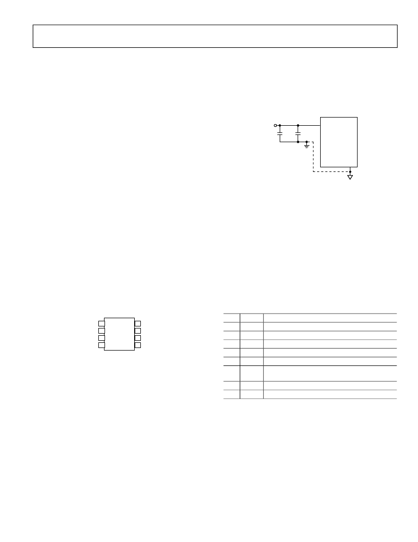
LAYOUT AND POWER SUPPLY BYPASSING
It is a good practice to employ compact, minimum lead length
layout design. The leads to the inputs should be as direct as
possible with a minimum conductor length. Ground paths
should have low resistance and low inductance.
Similarly, it is also a good practice to bypass the power supplies
with quality capacitors for optimum stability. Supply leads to the
device should be bypassed with disc or chip ceramic capacitors
of 0.01 μF to 0.1 μF. Low ESR 1 μF to 10 μF tantalum or
electrolytic capacitors should also be applied at the supplies to
minimize any transient disturbance and low frequency ripple
(see Figure 45). Note that the digital ground should also be
joined remotely to the analog ground at one point to minimize
the ground bounce.
AD5245
V
DD
C1
C3
GND
10
μ
F
0.1
μ
F
+
V
DD
Figure 45. Power Supply Bypassing
PIN CONFIGURATION AND FUNCTION DESCRIPTIONS
PIN CONFIGURATION
A
B
AD0
SDA
1
2
3
4
5
8
7
6
W
V
DD
GND
SCL
TOP VIEW
(Not to Scale)
AD5245
Figure 46.
PIN FUNCTION DESCRIPTIONS
Table 9.
Pin
Name
Description
1
W
W Terminal.
2
V
DD
Positive Power Supply.
3
GND
Digital Ground.
4
SCL
Serial Clock Input. Positive edge triggered.
5
SDA
Serial Data Input/Output.
6
AD0
Programmable address bit 0 for multiple
package decoding.
7
B
B Terminal.
8
A
A Terminal.
Rev. 0 | Page 15 of 16
相关PDF资料 |
PDF描述 |
|---|---|
| AD5245BRJ100-RL7 | 256-Position I2C Compatible Digital Potentiometer |
| AD5245BRJ50-R2 | 256-Position I2C Compatible Digital Potentiometer |
| AD5245BRJ50-RL7 | 256-Position I2C Compatible Digital Potentiometer |
| AD5245EVAL | 256-Position I2C Compatible Digital Potentiometer |
| AD5246 | 128-Position I2C Compatible Digital Resistor |
相关代理商/技术参数 |
参数描述 |
|---|---|
| AD5245BRJ100-RL7 | 制造商:AD 制造商全称:Analog Devices 功能描述:256-Position I2C Compatible Digital Potentiometer |
| AD5245BRJ10-R2 | 制造商:Analog Devices 功能描述:IC DIGITAL POT. 8-BIT I2C |
| AD5245BRJ10-RL7 | 制造商:Analog Devices 功能描述:Digital Potentiometer 256POS 10KOhm Single 8-Pin SOT-23 T/R |
| AD5245BRJ5 | 制造商:AD 制造商全称:Analog Devices 功能描述:256-Position I2C-Compatible Digital Potentiometer |
| AD5245BRJ50 | 制造商:AD 制造商全称:Analog Devices 功能描述:256-Position I2C-Compatible Digital Potentiometer |
发布紧急采购,3分钟左右您将得到回复。