参数资料
| 型号: | AD524BE |
| 厂商: | Analog Devices Inc |
| 文件页数: | 10/28页 |
| 文件大小: | 0K |
| 描述: | IC AMP INST 1MHZ PREC LN 20CLCC |
| 标准包装: | 1 |
| 放大器类型: | 仪表 |
| 电路数: | 1 |
| 转换速率: | 5 V/µs |
| 增益带宽积: | 1MHz |
| -3db带宽: | 1MHz |
| 电流 - 输入偏压: | 25nA |
| 电压 - 输入偏移: | 100µV |
| 电流 - 电源: | 3.5mA |
| 电压 - 电源,单路/双路(±): | ±6 V ~ 18 V |
| 工作温度: | -25°C ~ 85°C |
| 安装类型: | 表面贴装 |
| 封装/外壳: | 20-CLCC |
| 供应商设备封装: | 20-LCCC |
| 包装: | 管件 |
第1页第2页第3页第4页第5页第6页第7页第8页第9页当前第10页第11页第12页第13页第14页第15页第16页第17页第18页第19页第20页第21页第22页第23页第24页第25页第26页第27页第28页
AD524
Rev. F | Page 18 of 28
GROUNDING
Many data acquisition components have two or more ground
pins that are not connected together within the device. These
grounds must be tied together at one point, usually at the system
power-supply ground. Ideally, a single solid ground would be
desirable. However, because current flows through the ground
wires and etch stripes of the circuit cards, and because these
paths have resistance and inductance, hundreds of millivolts can
be generated between the system ground point and the data
acquisition components. Separate ground returns should be
provided to minimize the current flow in the path from the
sensitive points to the system ground point. In this way, supply
currents and logic-gate return currents are not summed into the
same return path as analog signals where they would cause
measurement errors.
Because the output voltage is developed with respect to the
potential on the reference terminal, an instrumentation
amplifier can solve many grounding problems.
DIGITAL P.S.
+5V
C
–15V
ANALOG P.S.
AD574A
C
+15V
6
AD524
AD583
SAMPLE
AND HOLD
DIG
COM
DIGITAL
DATA
OUTPUT
SIGNAL
GROUND
ANALOG
GROUND*
OUTPUT
REFERENCE
*IF INDEPENDENT; OTHERWISE, RETURN AMPLIFIER REFERENCE
TO MECCA AT ANALOG P.S. COMMON.
1F
1F 1F
0.1
F
0.1
F
0.1
F
0.1
F
2
1
8
7
10
9
7
9
11 15
1
00
50
0
-0
43
Figure 43. Basic Grounding Practice
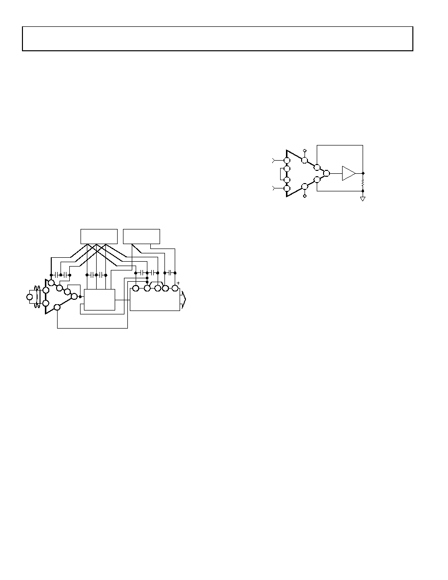
SENSE TERMINAL
The sense terminal is the feedback point for the instrument
amplifier’s output amplifier. Normally, it is connected to the
instrument amplifier output. If heavy load currents are to be
drawn through long leads, voltage drops due to current flowing
through lead resistance can cause errors. The sense terminal can
be wired to the instrument amplifier at the load, thus putting
the IxR drops inside the loop and virtually eliminating this
error source.
V–
V+
X1
AD524
(REF)
(SENSE)
OUTPUT
CURRENT
BOOSTER
RL
VIN+
VIN–
2
3
12
1
7
6
9
10
8
0050
0-
044
Figure 44. AD524 Instrumentation Amplifier with Output Current Booster
Typically, IC instrumentation amplifiers are rated for a full
±10 volt output swing into 2 kΩ. In some applications, however,
the need exists to drive more current into heavier loads.
Figure 44 shows how a high current booster may be connected
inside the loop of an instrumentation amplifier to provide the
required current boost without significantly degrading overall
performance. Nonlinearities and offset and gain inaccuracies of
the buffer are minimized by the loop gain of the AD524 output
amplifier. Offset drift of the buffer is similarly reduced.
REFERENCE TERMINAL
The reference terminal can be used to offset the output by up to
±10 V. This is useful when the load is floating or does not share
a ground with the rest of the system. It also provides a direct
means of injecting a precise offset. It must be remembered that
the total output swing is ±10 V to be shared between signal and
reference offset.
When the AD524 is of the 3-amplifier configuration it
is necessary that nearly zero impedance be presented to the
reference terminal.
Any significant resistance from the reference terminal to
ground increases the gain of the noninverting signal path,
thereby upsetting the common-mode rejection of the AD524.
In the AD524, a reference source resistance unbalances the CMR
trim by the ratio of 20 kΩ/RREF. For example, if the reference
source impedance is 1 Ω, CMR is reduced to 86 dB (20 kΩ/1 Ω
= 86 dB). An operational amplifier can be used to provide that
low impedance reference point, as shown in Figure 45. The
input offset voltage characteristics of that amplifier adds directly
to the output offset voltage performance of the instrumentation
amplifier.
相关PDF资料 |
PDF描述 |
|---|---|
| 3408-5003 | CONN HEADER 16POS R/A NO LATCH |
| AD204JN | IC AMP ISOL 5KHZ QUAD LP 38DIP |
| 3314-6303 | CONN HEADER 14POS STR LONG LATCH |
| AD204JY | IC AMP ISOL 5KHZ QUAD LP 38SIP |
| 350015-2 | CONN RECEPT 18-22 AWG .093 |
相关代理商/技术参数 |
参数描述 |
|---|---|
| AD524C | 制造商:AD 制造商全称:Analog Devices 功能描述:Precision Instrumentation Amplifier |
| AD524CD | 功能描述:IC AMP INST 1MHZ PREC LN 16CDIP RoHS:否 类别:集成电路 (IC) >> Linear - Amplifiers - Instrumentation 系列:- 其它有关文件:TS1854A View All Specifications 标准包装:50 系列:- 放大器类型:通用 电路数:4 输出类型:满摆幅 转换速率:0.25 V/µs 增益带宽积:630kHz -3db带宽:- 电流 - 输入偏压:16nA 电压 - 输入偏移:1000µV 电流 - 电源:162µA 电流 - 输出 / 通道:48mA 电压 - 电源,单路/双路(±):1.8 V ~ 6 V 工作温度:-40°C ~ 125°C 安装类型:表面贴装 封装/外壳:14-SOIC(0.154",3.90mm 宽) 供应商设备封装:14-SO 包装:管件 |
| AD524CD/+ | 制造商:未知厂家 制造商全称:未知厂家 功能描述:Instrumentation Amp, Pin-Programmable |
| AD524CDZ | 功能描述:IC AMP INST 1MHZ PREC LN 16CDIP RoHS:是 类别:集成电路 (IC) >> Linear - Amplifiers - Instrumentation 系列:- 标准包装:2,500 系列:- 放大器类型:通用 电路数:4 输出类型:- 转换速率:0.6 V/µs 增益带宽积:1MHz -3db带宽:- 电流 - 输入偏压:45nA 电压 - 输入偏移:2000µV 电流 - 电源:1.4mA 电流 - 输出 / 通道:40mA 电压 - 电源,单路/双路(±):3 V ~ 32 V,±1.5 V ~ 16 V 工作温度:0°C ~ 70°C 安装类型:表面贴装 封装/外壳:14-TSSOP(0.173",4.40mm 宽) 供应商设备封装:14-TSSOP 包装:带卷 (TR) 其它名称:LM324ADTBR2G-NDLM324ADTBR2GOSTR |
| AD524CE | 制造商:Rochester Electronics LLC 功能描述:- Bulk 制造商:Analog Devices 功能描述: |
发布紧急采购,3分钟左右您将得到回复。