参数资料
| 型号: | AD524CDZ |
| 厂商: | Analog Devices Inc |
| 文件页数: | 13/28页 |
| 文件大小: | 0K |
| 描述: | IC AMP INST 1MHZ PREC LN 16CDIP |
| 标准包装: | 1 |
| 放大器类型: | 仪表 |
| 电路数: | 1 |
| 转换速率: | 5 V/µs |
| 增益带宽积: | 1MHz |
| -3db带宽: | 1MHz |
| 电流 - 输入偏压: | 15nA |
| 电压 - 输入偏移: | 50µV |
| 电流 - 电源: | 3.5mA |
| 电压 - 电源,单路/双路(±): | ±6 V ~ 18 V |
| 工作温度: | -25°C ~ 85°C |
| 安装类型: | 通孔 |
| 封装/外壳: | 16-CDIP(0.300",7.62mm) |
| 供应商设备封装: | 16-CDIP 侧面铜焊 |
| 包装: | 管件 |
| 产品目录页面: | 770 (CN2011-ZH PDF) |
第1页第2页第3页第4页第5页第6页第7页第8页第9页第10页第11页第12页当前第13页第14页第15页第16页第17页第18页第19页第20页第21页第22页第23页第24页第25页第26页第27页第28页
AD524
Rev. F | Page 20 of 28
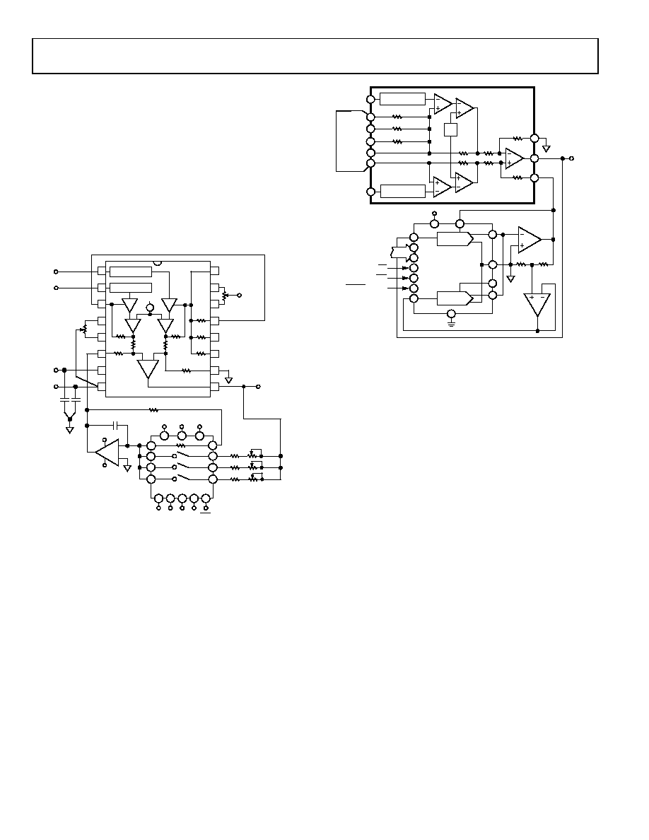
PROGRAMMABLE GAIN
Figure 47 shows the AD524 being used as a software program-
mable gain amplifier. Gain switching can be accomplished with
mechanical switches such as DIP switches or reed relays. It should
be noted that the on resistance of the switch in series with the
internal gain resistor becomes part of the gain equation and has
an effect on gain accuracy.
The AD524 can also be connected for gain in the output stage.
Figure 48 shows an AD711 used as an active attenuator in the
output amplifier’s feedback loop. The active attenuation presents
very low impedance to the feedback resistors, therefore
minimizing the common-mode rejection ratio degradation.
TO –V
AD524
1
2
3
4
5
6
7
8
16
15
14
13
12
11
10
9
20k
404
4.44k
20k
40
PROTECTION
–IN
+IN
(+INPUT)
(–INPUT)
10k
10pF
20k
AD711
AD7590
GND
39.2k
28.7k
316k
1k
A4
A3
A2
WR
–VS
+VS
1F
35V
INPUT
OFFSET
NULL
+VS
OUTPUT
OFFSET
NULL
R2
10k
VOUT
+VS
–VS
VDD
VSS VDD
15
13
11
9
2
14
12
10
34
5
67
18
16
00
50
0-
04
8
+
–
+
–
Figure 48. Programmable Output Gain
2
1
10
6
AD524
DAC A
DB0
256:1
20k
G = 10
G = 100
G = 1000
4.44k
404
40
PROTECTION
20k
DAC B
DB7
AD7528
9
16
11
12
PROTECTION
3
13
RG1
RG2
Vb
+INPUT
(–INPUT)
–INPUT
(+INPUT)
VOUT
CS
WR
1/2
AD712
1/2
AD712
DATA
INPUTS
DAC A/DAC B
+VS
4
14
7
15
16
6
18
5
17
3
2
1
19
20
0050
0-
0
49
Figure 49. Programmable Output Gain Using a DAC
Another method for developing the switching scheme is to
use a DAC. The AD7528 dual DAC, which acts essentially as
a pair of switched resistive attenuators having high analog
linearity and symmetrical bipolar transmission, is ideal in this
application. The multiplying DAC’s advantage is that it can
handle inputs of either polarity or zero without affecting the
programmed gain. The circuit shown uses an AD7528 to set
the gain (DAC A) and to perform a fine adjustment (DAC B).
AUTOZERO CIRCUITS
In many applications, it is necessary to provide very accurate
data in high gain configurations. At room temperature, the
offset effects can be nulled by the use of offset trim potenti-
ometers. Over the operating temperature range, however,
offset nulling becomes a problem. The circuit of Figure 50
shows a CMOS DAC operating in bipolar mode and connected
to the reference terminal to provide software controllable offset
adjustments.
相关PDF资料 |
PDF描述 |
|---|---|
| RMCF0603JT150R | RES 150 OHM 1/10W 5% 0603 SMD |
| RMCF0603JT2M20 | RES 2.2M OHM 1/10W 5% 0603 SMD |
| RMCF0603JT330K | RES 330K OHM 1/10W 5% 0603 SMD |
| UESD5.0DT5G | DIODE ESD PROTECT 5V SOT-723 |
| RMCF0603JT82K0 | RES 82K OHM 1/10W 5% 0603 SMD |
相关代理商/技术参数 |
参数描述 |
|---|---|
| AD524CE | 制造商:Rochester Electronics LLC 功能描述:- Bulk 制造商:Analog Devices 功能描述: |
| AD524S | 制造商:AD 制造商全称:Analog Devices 功能描述:Precision Instrumentation Amplifier |
| AD524SCHIPS | 制造商:AD 制造商全称:Analog Devices 功能描述:Precision Instrumentation Amplifier |
| AD524SD | 功能描述:IC AMP INST 1MHZ PREC LN 16CDIP RoHS:否 类别:集成电路 (IC) >> Linear - Amplifiers - Instrumentation 系列:- 标准包装:1 系列:- 放大器类型:通用 电路数:4 输出类型:满摆幅 转换速率:0.028 V/µs 增益带宽积:105kHz -3db带宽:- 电流 - 输入偏压:3nA 电压 - 输入偏移:100µV 电流 - 电源:3.3µA 电流 - 输出 / 通道:12mA 电压 - 电源,单路/双路(±):2.7 V ~ 12 V,±1.35 V ~ 6 V 工作温度:-40°C ~ 85°C 安装类型:表面贴装 封装/外壳:14-TSSOP(0.173",4.40mm 宽) 供应商设备封装:14-TSSOP 包装:剪切带 (CT) 其它名称:OP481GRUZ-REELCT |
| AD524SD/883B | 功能描述:仪表放大器 PRECISION LOW NOISE IN AM RoHS:否 制造商:Texas Instruments 通道数量: 输入补偿电压:150 V 可用增益调整: 最大输入电阻:10 kOhms 共模抑制比(最小值):88 dB 工作电源电压:2.7 V to 36 V 电源电流:200 uA 最大工作温度:+ 125 C 最小工作温度:- 40 C 封装 / 箱体:MSOP-8 封装:Bulk |
发布紧急采购,3分钟左右您将得到回复。