- 您现在的位置:买卖IC网 > PDF目录9287 > AD5254BRUZ50-RL7 (Analog Devices Inc)IC POT DGTL QUAD 50K 20TSSOP PDF资料下载
参数资料
| 型号: | AD5254BRUZ50-RL7 |
| 厂商: | Analog Devices Inc |
| 文件页数: | 15/32页 |
| 文件大小: | 0K |
| 描述: | IC POT DGTL QUAD 50K 20TSSOP |
| 标准包装: | 1,000 |
| 接片: | 256 |
| 电阻(欧姆): | 50k |
| 电路数: | 4 |
| 温度系数: | 标准值 650 ppm/°C |
| 存储器类型: | 非易失 |
| 接口: | I²C(设备位址) |
| 电源电压: | 2.7 V ~ 5.5 V,±2.25 V ~ 2.75 V |
| 工作温度: | -40°C ~ 85°C |
| 安装类型: | 表面贴装 |
| 封装/外壳: | 20-TSSOP(0.173",4.40mm 宽) |
| 供应商设备封装: | 20-TSSOP |
| 包装: | 带卷 (TR) |
第1页第2页第3页第4页第5页第6页第7页第8页第9页第10页第11页第12页第13页第14页当前第15页第16页第17页第18页第19页第20页第21页第22页第23页第24页第25页第26页第27页第28页第29页第30页第31页第32页
AD5253/AD5254
Data Sheet
Rev. C | Page 22 of 32
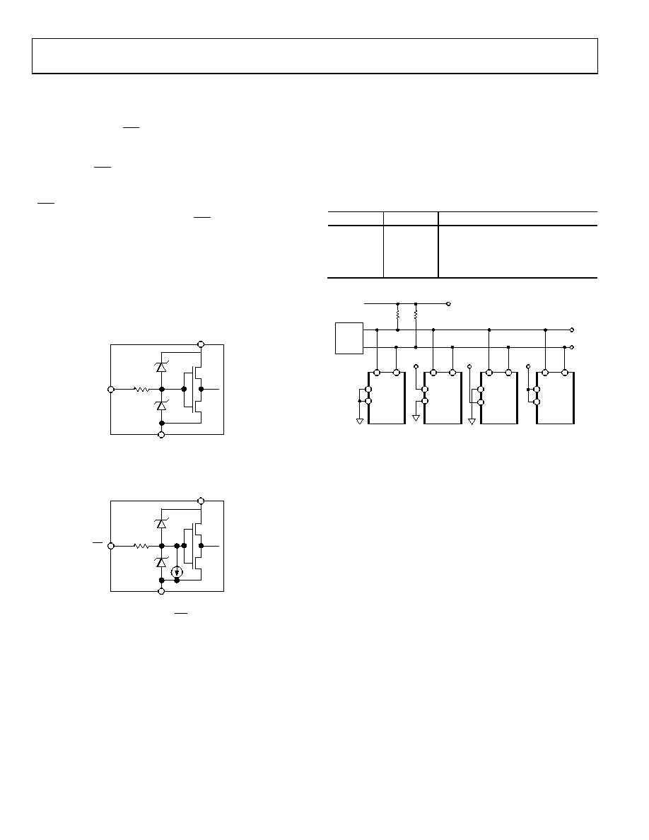
DIGITAL INPUT/OUTPUT CONFIGURATION
SDA is a digital input/output with an open-drain MOSFET that
requires a pull-up resistor for proper communication. On the
other hand, SCL and WP are digital inputs for which pull-up
resistors are recommended to minimize the MOSFET cross-
conduction current when the driving signals are lower than
VDD. SCL and WP have ESD protection diodes, as shown in
WP can be permanently tied to VDD without a pull-up resistor if
the write-protect feature is not used. If WP is left floating, an
internal current source pulls it low to enable write protection. In
applications in which the device is programmed infrequently,
this allows the part to default to write-protection mode after
any one-time factory programming or field calibration without
using an on-board pull-down resistor. Because there are
protection diodes on all inputs, the signal levels must not be
greater than VDD to prevent forward biasing of the diodes.
03824-0-035
GND
SCL
VDD
Figure 35. SCL Digital Input
03824-0-036
GND
INPUTS
WP
VDD
Figure 36. Equivalent WP Digital Input
MULTIPLE DEVICES ON ONE BUS
The AD5253/AD5254 are equipped with two addressing pins,
AD1 and AD0, that allow up to four AD5253/AD5254 devices
to be operated on one I2C bus. To achieve this result, the states of
AD1 and AD0 on each device must first be defined. An example
device is issued a different slave address—01011(AD1)(AD0)—
to complete the addressing.
Table 12. Multiple Devices Addressing
AD1
AD0
Device Addressed
0
U1
0
1
U2
1
0
U3
1
U4
SDA
AD1
AD0
MASTER
SCL
SDA
AD1
AD0
SCL
SDA
AD1
AD0
SCL
SDA
5V
RP
5V
AD1
AD0
SCL
AD5253/
AD5254
AD5253/
AD5254
AD5253/
AD5254
AD5253/
AD5254
03824-0-037
Figure 37. Multiple AD5253/AD5254 Devices on a Single Bus
In wireless base station smart-antenna systems that require
arrays of digital potentiometers to bias the power amplifiers,
large numbers of AD5253/AD5254 devices can be addressed by
using extra decoders, switches, and I/O buses, as shown in
Figure 38. For example, to communicate to a total of 16 devices,
four decoders and 16 sets of combinational switches (four sets
shown in Figure 38) are needed. Two I/O buses serve as the
common inputs of the four 2 × 4 decoders and select four sets
of outputs at each combination. Because the four sets of
combination switch outputs are unique, as shown in Figure 38,
a specific device is addressed by properly programming the I2C
with the slave address defined as 01011(AD1)(AD0). This
operation allows one of 16 devices to be addressed, provided
that the inputs of the two decoders do not change states. The
inputs of the decoders are allowed to change once the operation
of the specified device is completed.
相关PDF资料 |
PDF描述 |
|---|---|
| VI-B4Z-MY-F2 | CONVERTER MOD DC/DC 2V 20W |
| VE-B74-MW-B1 | CONVERTER MOD DC/DC 48V 100W |
| M83723/83R18146 | CONN RCPT 14POS WALL MT W/PINS |
| VI-B6M-IU-F1 | CONVERTER MOD DC/DC 10V 200W |
| VI-B4Z-MY-F1 | CONVERTER MOD DC/DC 2V 20W |
相关代理商/技术参数 |
参数描述 |
|---|---|
| AD5254EVAL | 制造商:Analog Devices 功能描述:EVAL BOARD FOR AD5254 - Bulk |
| AD5255 | 制造商:AD 制造商全称:Analog Devices 功能描述:3-Channel Digital Potentiometer with Nonvolatile Memory |
| AD5255BRU25 | 制造商:Analog Devices 功能描述:DGTL POTENTIOMETER 512POS 25KOHM TRIPLE 24TSSOP - Rail/Tube |
| AD5255BRU250 | 制造商:Analog Devices 功能描述:DGTL POTENTIOMETER 512POS 250KOHM TRIPLE 24TSSOP - Rail/Tube |
| AD5255BRU250-RL7 | 制造商:Analog Devices 功能描述:DGTL POTENTIOMETER 512POS 250KOHM TRIPLE 24TSSOP - Tape and Reel |
发布紧急采购,3分钟左右您将得到回复。