参数资料
| 型号: | AD5262BRUZ50 |
| 厂商: | Analog Devices Inc |
| 文件页数: | 13/24页 |
| 文件大小: | 0K |
| 描述: | IC POT DUAL 50K 256POS 16TSSOP |
| 标准包装: | 96 |
| 接片: | 256 |
| 电阻(欧姆): | 50k |
| 电路数: | 2 |
| 温度系数: | 标准值 35 ppm/°C |
| 存储器类型: | 易失 |
| 接口: | 4 线 SPI(芯片选择) |
| 电源电压: | 4.5 V ~ 16.5 V,±4.5 V ~ 5.5 V |
| 工作温度: | -40°C ~ 85°C |
| 安装类型: | 表面贴装 |
| 封装/外壳: | 16-TSSOP(0.173",4.40mm 宽) |
| 供应商设备封装: | 16-TSSOP |
| 包装: | 管件 |
| 产品目录页面: | 787 (CN2011-ZH PDF) |
AD5260/AD5262
Rev. A | Page 20 of 24
BIPOLAR PROGRAMMABLE GAIN AMPLIFIER
For applications that require bipolar gain, Figure 62 shows one
implementation. Digital Potentiometer U1 sets the adjustment
range. The wiper voltage at W2 can therefore be programmed
between Vi and KVi at a given U2 setting. Configuring A2 in
the noninverting mode allows linear gain and attenuation. The
transfer function is
()
+
×
+
=
K
D
R1
R2
V
i
O
1
256
2
1
(5)
where K is the ratio of RWB1/RWA1 set by U1.
–KVi
A1
B1
A2
R1
R2
VDD
VSS
VDD
OP2177
A2
B2
W2
U2
AD5262
U1
AD5262
W1
A1
VO
C1
Vi
02
695
-062
Figure 62. Bipolar Programmable Gain Amplifier
Similar to the previous example, in the simpler and more
common case, where K = 1, with a single digital potentiometer,
AD5260, U1 is replaced by a matched pair of resistors to apply
Vi and Vi at the ends of the digital potentiometer. The relation-
ship becomes
i
O
V
D
R1
R2
V
×
+
=
1
256
2
1
(6)
If R2 is large, a few picofarad compensation capacitors may be
needed to avoid any gain peaking.
Table 11 shows the result of adjusting D, with A2 configured as
a unity gain, a gain of 2, and a gain of 10. The result is a bipolar
amplifier with linearly programmable gain and 256-step
resolution.
Table 11. Result of Bipolar Gain Amplifier
D
R1 = ∞, R2 = 0
R1 = R2
R2 = 9 × R1
0
1
2
10
64
0.5
1
5
128
0
192
+0.5
+1
+5
255
+0.968
+1.937
+9.680
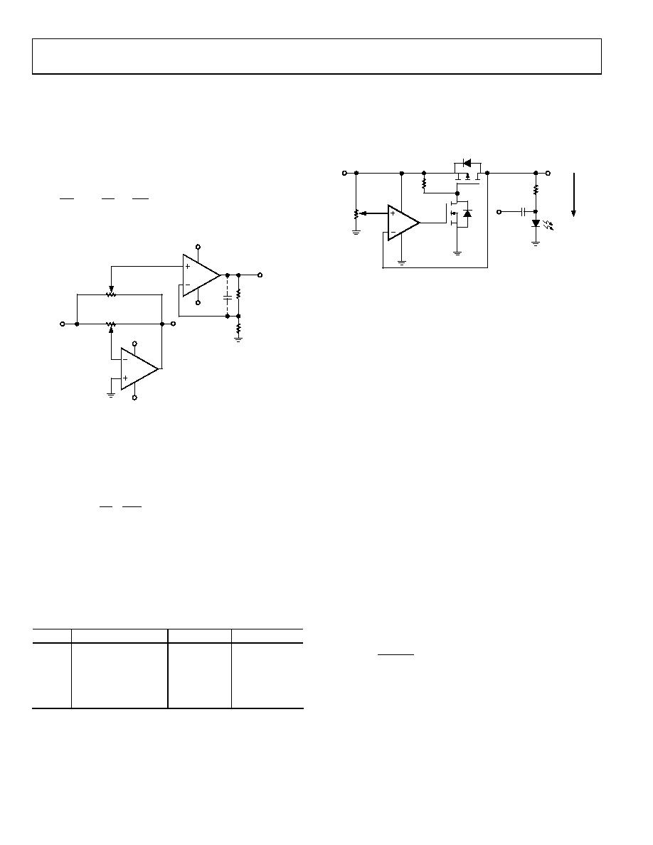
PROGRAMMABLE VOLTAGE SOURCE WITH
BOOSTED OUTPUT
For applications that require high current adjustment such as a
laser diode driver or tunable laser, a boosted voltage source can
be considered (see Figure 63).
Vi
A1
VO
W
U1
A
B
CC
IL
5V
SIGNAL LO
N1
R1
10k
P1
RBIAS
U1 = AD5260
A1 = AD8601, AD8605, AD8541
P1 = FDP360P, NDS9430
N1 = FDV301N, 2N7002
026
95-
0
63
Figure 63. Programmable Boosted Voltage Source
In this circuit, the inverting input of the op amp forces VO to be
equal to the wiper voltage set by the digital potentiometer. The
load current is then delivered by the supply via the P-channel
FET, P1. The N-channel FET, N1, simplifies the op amp driving
requirement. A1 must be the rail-to-rail input type. Resistor R1
is needed to prevent P1 from turning off once it is on. The choice
of R1 is a balance between the power loss of this resistor and
the output turn-off time. N1 can be any general-purpose signal
FET. However, P1 is driven in the saturation state, and there-
fore, its power handling must be adequate to dissipate (Vi VO)
× IL power. This circuit can source a maximum of 100 mA at 5 V
supply. Higher current can be achieved with P1 in a larger pack-
age. Note that a single N-channel FET can replace P1, N1, and
R1 altogether. However, the output swing is limited unless sepa-
rate power supplies are used. For a precision application, a
be applied at the input of the digital potentiometer.
PROGRAMMABLE 4 mA-TO-20 mA CURRENT
SOURCE
A programmable 4 mA-to-20 mA current source can be
unique low supply headroom and high current handling
precision reference that can deliver 20 mA at 2.048 V. The load
current is simply the voltage across Terminal B to Terminal W
of the digital potentiometer, divided by RS.
S
REF
L
R
D
V
I
×
=
(7)
相关PDF资料 |
PDF描述 |
|---|---|
| AD5262BRUZ20 | IC POT DUAL 20K 256POS 16TSSOP |
| 74LCX138M | DECODER/DEMUX 1OF8 5V 16-SOIC |
| VE-23V-MY-F3 | CONVERTER MOD DC/DC 5.8V 50W |
| VE-23V-MY-F2 | CONVERTER MOD DC/DC 5.8V 50W |
| VE-23T-MY-F4 | CONVERTER MOD DC/DC 6.5V 50W |
相关代理商/技术参数 |
参数描述 |
|---|---|
| AD5262BRUZ50 | 制造商:Analog Devices 功能描述:IC DIGITAL POT 50KOHM 256 DUAL 16-TSSO |
| AD5262BRUZ50-RL7 | 功能描述:IC POT DUAL 50K 256POS 16TSSOP RoHS:是 类别:集成电路 (IC) >> 数据采集 - 数字电位器 系列:- 标准包装:3,000 系列:DPP 接片:32 电阻(欧姆):10k 电路数:1 温度系数:标准值 300 ppm/°C 存储器类型:非易失 接口:3 线串行(芯片选择,递增,增/减) 电源电压:2.5 V ~ 6 V 工作温度:-40°C ~ 85°C 安装类型:表面贴装 封装/外壳:8-WFDFN 裸露焊盘 供应商设备封装:8-TDFN(2x3) 包装:带卷 (TR) |
| AD5262-EVAL | 制造商:Analog Devices 功能描述:EVAL KIT FOR 1-/2CH 15 V DGTL POTENTIOMETERS - Bulk |
| AD5263 | 制造商:AD 制造商全称:Analog Devices 功能描述:Preliminary Technical Data |
| AD5263_12 | 制造商:AD 制造商全称:Analog Devices 功能描述:Quad, 15 V, 256-Position, Digital Potentiometer with Pin-Selectable SPI/I2C |
发布紧急采购,3分钟左右您将得到回复。