参数资料
| 型号: | AD5262BRUZ50 |
| 厂商: | Analog Devices Inc |
| 文件页数: | 8/24页 |
| 文件大小: | 0K |
| 描述: | IC POT DUAL 50K 256POS 16TSSOP |
| 标准包装: | 96 |
| 接片: | 256 |
| 电阻(欧姆): | 50k |
| 电路数: | 2 |
| 温度系数: | 标准值 35 ppm/°C |
| 存储器类型: | 易失 |
| 接口: | 4 线 SPI(芯片选择) |
| 电源电压: | 4.5 V ~ 16.5 V,±4.5 V ~ 5.5 V |
| 工作温度: | -40°C ~ 85°C |
| 安装类型: | 表面贴装 |
| 封装/外壳: | 16-TSSOP(0.173",4.40mm 宽) |
| 供应商设备封装: | 16-TSSOP |
| 包装: | 管件 |
| 产品目录页面: | 787 (CN2011-ZH PDF) |
AD5260/AD5262
Rev. A | Page 16 of 24
RDAC1
RDAC2
AD5260/AD5262
SDI
CLK
CS
ADDR
DECODE
SERIAL
REGISTER
0
269
5-
0
49
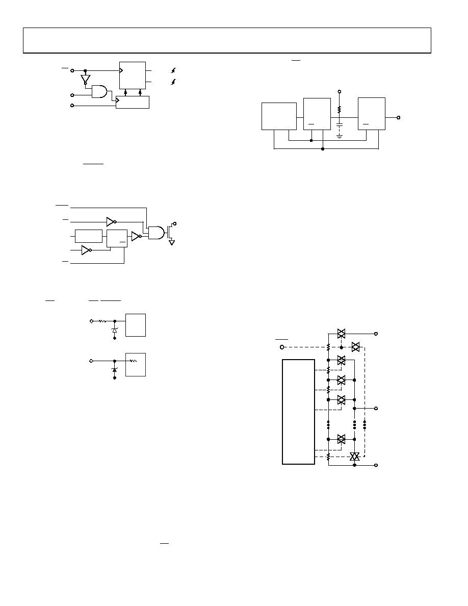
Figure 48. Equivalent Input Control Logic
The target RDAC latch is loaded with the last eight bits of
the serial data word completing one RDAC update. For the
AD5262, two separate 9-bit data words must be clocked in to
change both VR settings.
During shutdown (SHDN), the SDO output pin is forced to the
off (logic high) state to disable power dissipation in the pull-up
resistor. See
for the equivalent SDO output circuit
schematic.
SDI
CLK
CS
SHDN
PR
SERIAL
REGISTER
DQ
CK
RS
SDO
0
269
5-
05
0
Figure 49. Detail SDO Output Schematic of the AD5260
All digital inputs are protected with a series input resistor and
parallel Zener ESD structure as shown in Figure 50. This applies
to the CS, SDI, SDO, PR, SHDN, and CLK digital input pins.
340
LOGIC
0
269
5-
05
1
Figure 50. ESD Protection of Digital Pins
A, B, W
VSS
02695-
052
Figure 51. ESD Protection of Resistor Terminals
DAISY-CHAIN OPERATION
The serial data output (SDO) pin contains an open-drain N-
channel FET. This output requires a pull-up resistor to transfer
data to the SDI pin of the next package. This allows for daisy-
chaining several RDACs from a single processor serial data line.
The pull-up resistor termination voltage can be larger than the
VDD supply voltage. It is recommended to increase the clock
period when using a pull-up resistor to the SDI pin of the
following device in series because capacitive loading at the
daisy-chain node connecting SDO and SDI between devices
may induce time delay to subsequent devices. Users should
be aware of this potential problem to achieve data transfer
successfully (see Figure 52). If two AD5260s are daisy-chained,
this requires a total of 16 bits of data. The first eight bits, complying
with the format shown in Table 2, go to U2, and the second
eight bits with the same format go to U1. The CS pin should be
kept low until all 16 bits are clocked into their respective serial
registers, and the CS pin is then pulled high to complete the
operation.
VDD
CS CLK
SDO
SDI
MOSI
MICRO-
CONTROLLER
SCLK
SS
RP
2.2k
AD5260
U1
U2
026
95-
05
5
CS CLK
SDO
SDI
Figure 52. Daisy-Chain Configuration
RDAC STRUCTURE
The RDAC contains a string of equal resistor segments with an
array of analog switches that act as the wiper connection. The
number of positions is the resolution of the device. The AD5260/
AD5262 have 256 connection points, allowing it to provide better
than 0.4% settability resolution. Figure 53 shows an equivalent
structure of the connections between the three terminals that
make up one channel of the RDAC. SWA and SWB are always
on, while one of the switches SW(0) to SW(2N – 1) is on one at a
time, depending on the resistance position decoded from the
data bits. Because the switch is not ideal, there is a 60 Ω wiper
resistance, RW. Wiper resistance is a function of supply voltage
and temperature. The lower the supply voltage is, the higher the
wiper resistance becomes. Similarly, the higher the temperature
is, the higher the wiper resistance becomes. Users should be
aware of the contribution of the wiper resistance when accurate
prediction of the output resistance is needed.
D7
D6
D5
D4
D3
D2
D1
D0
RDAC
LATCH
AND
DECODE
Ax
Wx
Bx
RS = RAB/2N
RS
SHDN
DIGITAL CIRCUITRY
OMITTED FOR CLARITY
0269
5-
056
Figure 53. Simplified RDAC Architecture
PROGRAMMING THE VARIABLE RESISTOR
Rheostat Operation
The nominal resistances of the RDAC between Terminal A and
Terminal B are available with values of 20 kΩ, 50 kΩ, and 200 kΩ.
The final three digits of the part number determine the nominal
resistance value, for example, 20 kΩ = 20, 50 kΩ = 50, 200 kΩ =
200. The nominal resistance (RAB) of the VR has 256 contact points
相关PDF资料 |
PDF描述 |
|---|---|
| AD5262BRUZ20 | IC POT DUAL 20K 256POS 16TSSOP |
| 74LCX138M | DECODER/DEMUX 1OF8 5V 16-SOIC |
| VE-23V-MY-F3 | CONVERTER MOD DC/DC 5.8V 50W |
| VE-23V-MY-F2 | CONVERTER MOD DC/DC 5.8V 50W |
| VE-23T-MY-F4 | CONVERTER MOD DC/DC 6.5V 50W |
相关代理商/技术参数 |
参数描述 |
|---|---|
| AD5262BRUZ50 | 制造商:Analog Devices 功能描述:IC DIGITAL POT 50KOHM 256 DUAL 16-TSSO |
| AD5262BRUZ50-RL7 | 功能描述:IC POT DUAL 50K 256POS 16TSSOP RoHS:是 类别:集成电路 (IC) >> 数据采集 - 数字电位器 系列:- 标准包装:3,000 系列:DPP 接片:32 电阻(欧姆):10k 电路数:1 温度系数:标准值 300 ppm/°C 存储器类型:非易失 接口:3 线串行(芯片选择,递增,增/减) 电源电压:2.5 V ~ 6 V 工作温度:-40°C ~ 85°C 安装类型:表面贴装 封装/外壳:8-WFDFN 裸露焊盘 供应商设备封装:8-TDFN(2x3) 包装:带卷 (TR) |
| AD5262-EVAL | 制造商:Analog Devices 功能描述:EVAL KIT FOR 1-/2CH 15 V DGTL POTENTIOMETERS - Bulk |
| AD5263 | 制造商:AD 制造商全称:Analog Devices 功能描述:Preliminary Technical Data |
| AD5263_12 | 制造商:AD 制造商全称:Analog Devices 功能描述:Quad, 15 V, 256-Position, Digital Potentiometer with Pin-Selectable SPI/I2C |
发布紧急采购,3分钟左右您将得到回复。