参数资料
| 型号: | AD526ADZ |
| 厂商: | Analog Devices Inc |
| 文件页数: | 13/14页 |
| 文件大小: | 0K |
| 描述: | IC AMP PGA 10MA 16CDIP |
| 标准包装: | 23 |
| 放大器类型: | 可编程增益 |
| 电路数: | 1 |
| 转换速率: | 24 V/µs |
| -3db带宽: | 4MHz |
| 电流 - 输入偏压: | 50pA |
| 电压 - 输入偏移: | 250µV |
| 电流 - 电源: | 10mA |
| 电流 - 输出 / 通道: | 10mA |
| 电压 - 电源,单路/双路(±): | ±4.5 V ~ 16.5 V |
| 工作温度: | -40°C ~ 85°C |
| 安装类型: | 通孔 |
| 封装/外壳: | 16-CDIP(0.300",7.62mm) |
| 供应商设备封装: | 16-CDIP 侧面铜焊 |
| 包装: | 管件 |
| 产品目录页面: | 770 (CN2011-ZH PDF) |
AD526
REV. D
–8–
THEORY OF OPERATION
The AD526 is a complete software programmable gain amplifier
(SPGA) implemented monolithically with a drift-trimmed
BiFET amplifier, a laser wafer trimmed resistor network, JFET
analog switches and TTL compatible gain code latches.
A particular gain is selected by applying the appropriate gain
code (see Table I) to the control logic. The control logic turns
on the JFET switch that connects the correct tap on the gain
network to the inverting input of the amplifier; all unselected
JFET gain switches are off (open). The “on” resistance of the
gain switches causes negligible gain error since only the
amplifier’s input bias current, which is less than 150 pA, actu-
ally flows through these switches.
The AD526 is capable of storing the gain code, (latched mode),
B, A0, A1, A2, under the direction of control inputs
CLK and
CS. Alternatively, the AD526 can respond directly to gain code
changes if the control inputs are tied low (transparent mode).
For gains of 8 and 16, a fraction of the frequency compensation
capacitance (C1 in Figure 32) is automatically switched out of
the circuit. This increases the amplifier’s bandwidth and im-
proves its signal settling time and slew rate.
AMPLIFIER
+VS
VIN
N1
N2
C1
C2
OUT
FORCE
OUT
SENSE
–VS
A0
A1
A2
B
CLK
CS
DIGITAL
GND
L
A
T
C
H
E
S
C
O
N
T
R
O
L
O
G
I
C
G = 8
G = 16
ANALOG
GND2
ANALOG
GND1
1k
1.7k
G = 2
G = 4
1.7k
3.4k
1k
14k
RESISTOR
NETWORK
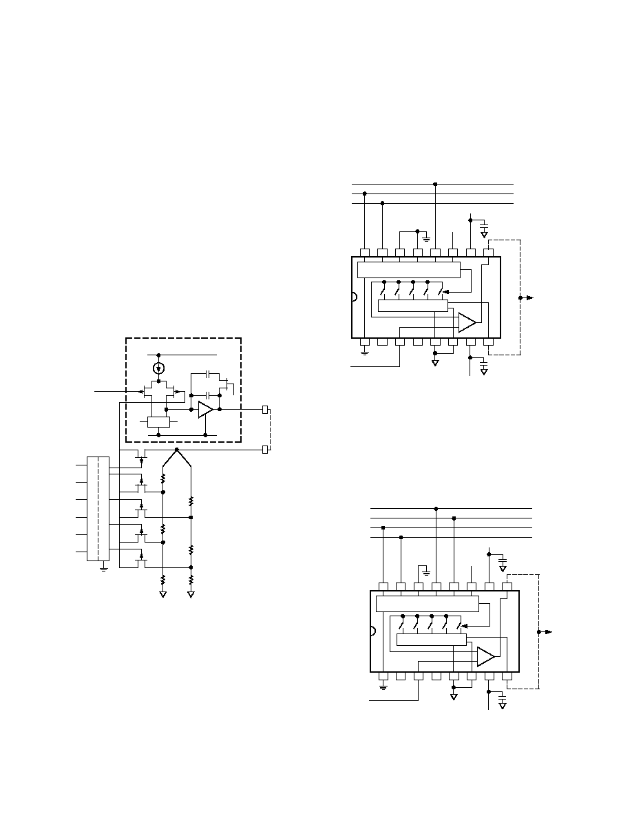
Figure 32. Simplified Schematic of the AD526
TRANSPARENT MODE OF OPERATION
In the transparent mode of operation, the AD526 will respond
directly to level changes at the gain code inputs (A0, A1, A2) if
B is tied high and both
CS and CLK are allowed to float low.
After the gain codes are changed, the AD526’s output voltage
typically requires 5.5
s to settle to within 0.01% of the final
value. Figures 26 to 29 show the performance of the AD526 for
positive gain code changes.
16
15
14
13
12
11
10
9
12
34
56
78
+
–
OUT
FORCE
OUT
SENSE
VOUT
0.1 F
AD526
16
84
21
GAIN NETWORK
A1
A0
CS CLK
A2
B
LOGIC AND LATCHES
–VS
0.1 F
+VS
+5V
A2
A1
A0
VIN
Figure 33. Transparent Mode
LATCHED MODE OF OPERATION
The latched mode of operation is shown in Figure 34. When
either
CS or CLK go to a Logic “1,” the gain code (A0, A1, A2,
B) signals are latched into the registers and held until both
CS
and
CLK return to “0.” Unused CS or CLK inputs should be tied
to ground . The
CS and CLK inputs are functionally and electri-
cally equivalent.
OUT
FORCE
OUT
SENSE
VOUT
0.1 F
–VS
0.1 F
+VS
+5V
A2
A1
A0
VIN
TIMING SIGNAL
16
15
14
13
12
11
10
9
12
34
56
78
+
–
AD526
16
84
21
GAIN NETWORK
A1
A0
CS CLK
A2
B
LOGIC AND LATCHES
Figure 34. Latched Mode
相关PDF资料 |
PDF描述 |
|---|---|
| 53324-0560 | CONN HEADER 2MM 5POS PCB TIN |
| OP470EY | IC OPAMP GP 6MHZ QUAD LN 14CDIP |
| 929836-02-04-RK | CONN HEADER .100 DUAL STR 8POS |
| OP400EY | IC OPAMP GP 500KHZ QUAD 14CDIP |
| 929835-01-26-RK | CONN HEADER .100 SNGL R/A 26POS |
相关代理商/技术参数 |
参数描述 |
|---|---|
| AD526B | 制造商:AD 制造商全称:Analog Devices 功能描述:Software Programmable Gain Amplifier |
| AD526BD | 功能描述:IC AMP PGA 10MA 16CDIP RoHS:否 类别:集成电路 (IC) >> Linear - Amplifiers - Instrumentation 系列:- 标准包装:2,500 系列:Excalibur™ 放大器类型:J-FET 电路数:1 输出类型:- 转换速率:45 V/µs 增益带宽积:10MHz -3db带宽:- 电流 - 输入偏压:20pA 电压 - 输入偏移:490µV 电流 - 电源:1.7mA 电流 - 输出 / 通道:48mA 电压 - 电源,单路/双路(±):4.5 V ~ 38 V,±2.25 V ~ 19 V 工作温度:-40°C ~ 85°C 安装类型:表面贴装 封装/外壳:8-SOIC(0.154",3.90mm 宽) 供应商设备封装:8-SOIC 包装:带卷 (TR) |
| AD526BDZ | 功能描述:IC AMP PGA 10MA 16CDIP RoHS:是 类别:集成电路 (IC) >> Linear - Amplifiers - Instrumentation 系列:- 标准包装:2,500 系列:- 放大器类型:通用 电路数:4 输出类型:- 转换速率:0.6 V/µs 增益带宽积:1MHz -3db带宽:- 电流 - 输入偏压:45nA 电压 - 输入偏移:2000µV 电流 - 电源:1.4mA 电流 - 输出 / 通道:40mA 电压 - 电源,单路/双路(±):3 V ~ 32 V,±1.5 V ~ 16 V 工作温度:0°C ~ 70°C 安装类型:表面贴装 封装/外壳:14-TSSOP(0.173",4.40mm 宽) 供应商设备封装:14-TSSOP 包装:带卷 (TR) 其它名称:LM324ADTBR2G-NDLM324ADTBR2GOSTR |
| AD526C | 制造商:AD 制造商全称:Analog Devices 功能描述:Software Programmable Gain Amplifier |
| AD526CD | 功能描述:IC AMP PGA 10MA 16CDIP RoHS:否 类别:集成电路 (IC) >> Linear - Amplifiers - Instrumentation 系列:- 标准包装:2,500 系列:- 放大器类型:通用 电路数:1 输出类型:满摆幅 转换速率:0.11 V/µs 增益带宽积:350kHz -3db带宽:- 电流 - 输入偏压:4nA 电压 - 输入偏移:20µV 电流 - 电源:260µA 电流 - 输出 / 通道:20mA 电压 - 电源,单路/双路(±):2.7 V ~ 36 V,±1.35 V ~ 18 V 工作温度:-40°C ~ 85°C 安装类型:表面贴装 封装/外壳:8-SOIC(0.154",3.90mm 宽) 供应商设备封装:8-SO 包装:带卷 (TR) |
发布紧急采购,3分钟左右您将得到回复。