参数资料
| 型号: | AD526ADZ |
| 厂商: | Analog Devices Inc |
| 文件页数: | 3/14页 |
| 文件大小: | 0K |
| 描述: | IC AMP PGA 10MA 16CDIP |
| 标准包装: | 23 |
| 放大器类型: | 可编程增益 |
| 电路数: | 1 |
| 转换速率: | 24 V/µs |
| -3db带宽: | 4MHz |
| 电流 - 输入偏压: | 50pA |
| 电压 - 输入偏移: | 250µV |
| 电流 - 电源: | 10mA |
| 电流 - 输出 / 通道: | 10mA |
| 电压 - 电源,单路/双路(±): | ±4.5 V ~ 16.5 V |
| 工作温度: | -40°C ~ 85°C |
| 安装类型: | 通孔 |
| 封装/外壳: | 16-CDIP(0.300",7.62mm) |
| 供应商设备封装: | 16-CDIP 侧面铜焊 |
| 包装: | 管件 |
| 产品目录页面: | 770 (CN2011-ZH PDF) |
AD526
REV. D
–11–
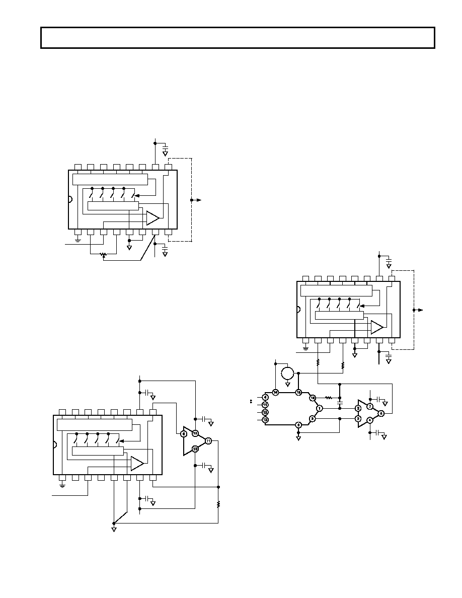
OFFSET NULLING
Input voltage offset nulling of the AD526 is best accomplished
at a gain of 16, since the referred-to-input (RTI) offset is ampli-
fied the most at this gain and therefore is most easily trimmed.
The resulting trimmed value of RTI voltage offset typically
varies less than 3
V across all gain ranges.
Note that the low input current of the AD526 minimizes RTI
voltage offsets due to source resistance.
OUT
FORCE
OUT
SENSE
VOUT
0.1 F
–VS
0.1 F
+VS
VIN
16
15
14
13
12
11
10
9
12
34
56
78
+
–
AD526
16
84
21
GAIN NETWORK
A1
A0
CS CLK
A2
B
LOGIC AND LATCHES
20k
Figure 39. Offset Voltage Null Circuit
OUTPUT CURRENT BOOSTER
The AD526 is rated for a full
±10 V output voltage swing into
2 k
. In some applications, the need exists to drive more cur-
rent into heavier loads. As shown in Figure 40, a high current
booster may be connected “inside the loop” of the SPGA to
provide the required current boost without significantly degrad-
ing overall performance. Nonlinearities, offset and gain inaccu-
racies of the buffer are minimized by the loop gain of the
AD526 output amplifier.
OUT
FORCE
OUT
SENSE
–VS
0.1 F
+VS
VIN
16
15
14
13
12
11
10
9
12
34
56
78
+
–
AD526
16
84
21
GAIN NETWORK
A1
A0
CS CLK
A2
B
LOGIC AND LATCHES
HOS-100
0.01 F
0.1 F
0.01 F
RL
Figure 40. Current Output Boosting
CASCADED OPERATION
A cascade of two AD526s can be used to achieve binarily
weighted gains from 1 to 256. If gains from 1 to 128 are needed,
no additional components are required. This is accomplished by
using the B pin as shown in Figure 38. When the B pin is low,
the AD526 is held in a unity gain stage independent of the other
gain code values.
OFFSET NULLING WITH A D/A CONVERTER
Figure 41 shows the AD526 with offset nulling accomplished
with an 8-bit D/A converter (AD7524) circuit instead of the
potentiometer shown in Figure 39. The calibration procedure is
the same as before except that instead of adjusting the potenti-
ometer, the D/A converter corrects for the offset error. This
calibration circuit has a number of benefits in addition to elimi-
nating the trimpot. The most significant benefit is that calibra-
tion can be under the control of a microprocessor and therefore
can be implemented as part of an autocalibration scheme. Sec-
ondly, dip switches or RAM can be used to hold the 8-bit word
after its value has been determined. In Figure 42 the offset null
sensitivity, at a gain of 16, is 80
V per LSB of adjustment,
which guarantees dc accuracy to the 16-bit performance level.
OUT
FORCE
OUT
SENSE
VOUT
0.1 F
–VS
0.1 F
+VS
VIN
16
15
14
13
12
11
10
9
1
2
34
56
7
8
+
–
AD526
16
84
21
GAIN NETWORK
A1
A0
CS CLK
A2
B
LOGIC AND LATCHES
AD581 OR
AD587
+10V
VREF
7.5M
3.3M
AD548
0.01 F
–
+
+VS
–VS
ALL BYPASS CAPACITORS ARE 0.1 F
AD7524
GND
10 F
1k
OUT 1
OUT 2
+VS
MSB
LSB
CS
WR
Figure 41. Offset Nulling Using a DAC
相关PDF资料 |
PDF描述 |
|---|---|
| 53324-0560 | CONN HEADER 2MM 5POS PCB TIN |
| OP470EY | IC OPAMP GP 6MHZ QUAD LN 14CDIP |
| 929836-02-04-RK | CONN HEADER .100 DUAL STR 8POS |
| OP400EY | IC OPAMP GP 500KHZ QUAD 14CDIP |
| 929835-01-26-RK | CONN HEADER .100 SNGL R/A 26POS |
相关代理商/技术参数 |
参数描述 |
|---|---|
| AD526B | 制造商:AD 制造商全称:Analog Devices 功能描述:Software Programmable Gain Amplifier |
| AD526BD | 功能描述:IC AMP PGA 10MA 16CDIP RoHS:否 类别:集成电路 (IC) >> Linear - Amplifiers - Instrumentation 系列:- 标准包装:2,500 系列:Excalibur™ 放大器类型:J-FET 电路数:1 输出类型:- 转换速率:45 V/µs 增益带宽积:10MHz -3db带宽:- 电流 - 输入偏压:20pA 电压 - 输入偏移:490µV 电流 - 电源:1.7mA 电流 - 输出 / 通道:48mA 电压 - 电源,单路/双路(±):4.5 V ~ 38 V,±2.25 V ~ 19 V 工作温度:-40°C ~ 85°C 安装类型:表面贴装 封装/外壳:8-SOIC(0.154",3.90mm 宽) 供应商设备封装:8-SOIC 包装:带卷 (TR) |
| AD526BDZ | 功能描述:IC AMP PGA 10MA 16CDIP RoHS:是 类别:集成电路 (IC) >> Linear - Amplifiers - Instrumentation 系列:- 标准包装:2,500 系列:- 放大器类型:通用 电路数:4 输出类型:- 转换速率:0.6 V/µs 增益带宽积:1MHz -3db带宽:- 电流 - 输入偏压:45nA 电压 - 输入偏移:2000µV 电流 - 电源:1.4mA 电流 - 输出 / 通道:40mA 电压 - 电源,单路/双路(±):3 V ~ 32 V,±1.5 V ~ 16 V 工作温度:0°C ~ 70°C 安装类型:表面贴装 封装/外壳:14-TSSOP(0.173",4.40mm 宽) 供应商设备封装:14-TSSOP 包装:带卷 (TR) 其它名称:LM324ADTBR2G-NDLM324ADTBR2GOSTR |
| AD526C | 制造商:AD 制造商全称:Analog Devices 功能描述:Software Programmable Gain Amplifier |
| AD526CD | 功能描述:IC AMP PGA 10MA 16CDIP RoHS:否 类别:集成电路 (IC) >> Linear - Amplifiers - Instrumentation 系列:- 标准包装:2,500 系列:- 放大器类型:通用 电路数:1 输出类型:满摆幅 转换速率:0.11 V/µs 增益带宽积:350kHz -3db带宽:- 电流 - 输入偏压:4nA 电压 - 输入偏移:20µV 电流 - 电源:260µA 电流 - 输出 / 通道:20mA 电压 - 电源,单路/双路(±):2.7 V ~ 36 V,±1.35 V ~ 18 V 工作温度:-40°C ~ 85°C 安装类型:表面贴装 封装/外壳:8-SOIC(0.154",3.90mm 宽) 供应商设备封装:8-SO 包装:带卷 (TR) |
发布紧急采购,3分钟左右您将得到回复。