- 您现在的位置:买卖IC网 > PDF目录9426 > AD5282BRUZ200 (Analog Devices Inc)IC DUAL POT 200K 256POS 16-TSSOP PDF资料下载
参数资料
| 型号: | AD5282BRUZ200 |
| 厂商: | Analog Devices Inc |
| 文件页数: | 6/28页 |
| 文件大小: | 0K |
| 描述: | IC DUAL POT 200K 256POS 16-TSSOP |
| 标准包装: | 96 |
| 接片: | 256 |
| 电阻(欧姆): | 200k |
| 电路数: | 2 |
| 温度系数: | 标准值 30 ppm/°C |
| 存储器类型: | 易失 |
| 接口: | I²C(设备位址) |
| 电源电压: | 4.5 V ~ 16.5 V,±4.5 V ~ 5.5 V |
| 工作温度: | -40°C ~ 85°C |
| 安装类型: | 表面贴装 |
| 封装/外壳: | 16-TSSOP(0.173",4.40mm 宽) |
| 供应商设备封装: | 16-TSSOP |
| 包装: | 管件 |
| 产品目录页面: | 787 (CN2011-ZH PDF) |
第1页第2页第3页第4页第5页当前第6页第7页第8页第9页第10页第11页第12页第13页第14页第15页第16页第17页第18页第19页第20页第21页第22页第23页第24页第25页第26页第27页第28页
AD5280/AD5282
Rev. C | Page 14 of
28
THEORY OF OPERATION
The AD5280/AD5282 are single-channel and dual-channel,
256-position, digitally controlled variable resistors (VRs). To
program the VR settings, see the Digital Interface section. Both
parts have an internal power-on preset that places the wiper at
midscale during power-on, which simplifies the fault condition
recovery at power-up. Operation of the power-on preset function
also depends on the state of the VL pin.
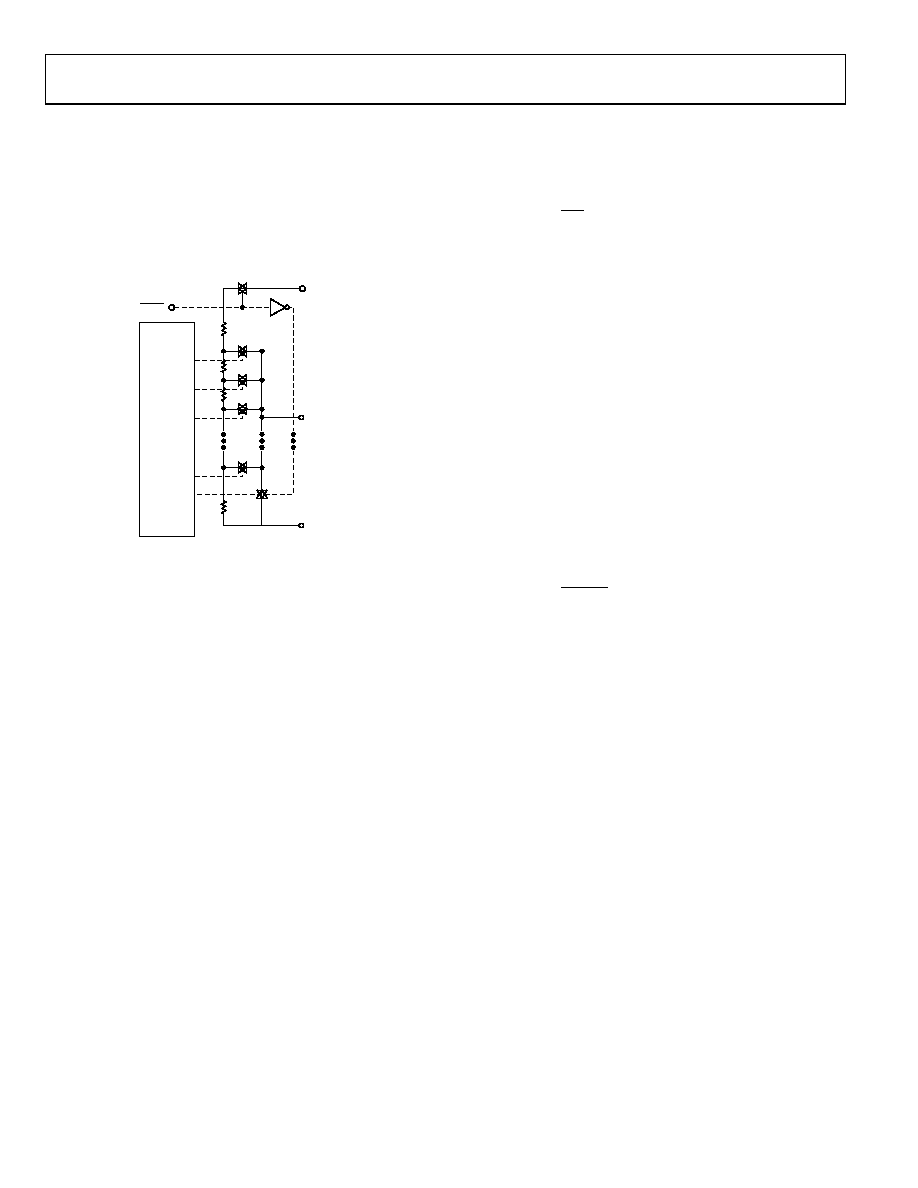
D7
D6
D5
D4
D3
D2
D1
D0
RDAC
LATCH
AND
DECODER
RS
AX
WX
RS
BX
SHDN
0xFF
0x01
SWB
SWA
0x00
5
02
92
9-
04
()
Figure 44. AD5280/AD5282 Equivalent RDAC Circuit
RHEOSTAT OPERATION
The nominal resistance of the RDAC between Terminal A and
Terminal B is available in 20 kΩ, 50 kΩ, and 200 kΩ. The final
two or three digits of the part number determine the nominal
resistance value, for example, 20 kΩ = 20, 50 kΩ = 50, and
200 kΩ = 200. The nominal resistance (RAB) of the VR has
256 contact points accessed by the wiper terminal, plus the B
terminal contact. The eight-bit data in the RDAC latch is
decoded to select one of the 256 possible settings. Assuming
that a 20 kΩ part is used, the wiper’s first connection starts at
the B terminal for data 0x00. Because there is a 60 Ω wiper
contact resistance, such a connection yields a minimum of 60 Ω
resistance between Terminal W and Terminal B.
The second connection is the first tap point that corresponds to
138 Ω (RWB = RAB/256 + RW = 78 Ω + 60 Ω) for data 0x01. The
third connection is the next tap point representing 216 Ω (78 ×
2 + 60) for data 0x02, and so on. Each LSB data value increase
moves the wiper up the resistor ladder until the last tap point is
simplified diagram of the equivalent RDAC circuit where the
last resistor string is not accessed; therefore, there is 1 LSB less
of the nominal resistance at full scale in addition to the wiper
resistance.
The general equation determining the digitally programmed
output resistance between W and B is
W
AB
WB
R
D
R
+
×
=
256
()
(1)
where:
D
is the decimal equivalent of the binary code loaded in the 8-
bit RDAC register.
RAB
is the nominal end-to-end resistance.
RW
is the wiper resistance contributed by the on resistance of
the internal switch.
Note that in the zero-scale condition, a finite wiper resistance
of 60 Ω is present. Care should be taken to limit the current
flow between W and B in this state to a maximum pulse current
of no more than 20 mA. Otherwise, degradation or possible
destruction of the internal switch contact can occur.
As in the mechanical potentiometer, the resistance of the RDAC
between Wiper W and Terminal A also produces a digitally
controlled complementary resistance, RWA. When these terminals
are used, the B terminal can be opened. Setting the resistance
value for RWA starts at a maximum value of resistance and
decreases as the data loaded in the latch increases in value. The
general equation for this operation is
W
AB
WA
R
D
R
+
×
=
256
(2)
The typical distribution of the nominal resistance, RAB, from
channel to channel matches within ±1%. Device-to-device
matching is process lot dependent, and it is possible to have a
±30% variation. Because the resistance element is processed in
thin film technology, the change in RAB with temperature is very
small (30 ppm/°C).
POTENTIOMETER OPERATION
The digital potentiometer easily generates a voltage divider at
wiper to B and wiper to A to be proportional to the input voltage
at A to B. Unlike the polarity of VDD – VSS, which must be
positive, voltage across A to B, W to A, and W to B can be at
either polarity, provided that VSS is powered by a negative supply.
If the effect of the wiper resistance for approximation is ignored,
connecting the A terminal to 5 V and the B terminal to ground
produces an output voltage at the wiper to B starting at 0 V up
to 1 LSB less than 5 V. Each LSB of voltage is equal to the
voltage applied across A to B divided by the 256 positions of the
potentiometer divider. Because the AD5280/AD5282 can be
supplied by dual supplies, the general equation defining the
output voltage at VW with respect to ground for any valid
相关PDF资料 |
PDF描述 |
|---|---|
| AD5282BRUZ20 | IC DUAL POT 20K 256POS 16-TSSOP |
| VE-23X-MY-F1 | CONVERTER MOD DC/DC 5.2V 50W |
| VE-23W-MY-F4 | CONVERTER MOD DC/DC 5.5V 50W |
| VE-23W-MY-F2 | CONVERTER MOD DC/DC 5.5V 50W |
| VE-23V-MY-F4 | CONVERTER MOD DC/DC 5.8V 50W |
相关代理商/技术参数 |
参数描述 |
|---|---|
| AD5282BRUZ2002 | 制造商:AD 制造商全称:Analog Devices 功能描述:Single/Dual,15 V/5 V,256-Position I2C-Compatible Digital Potentiometer |
| AD5282BRUZ200-R7 | 功能描述:IC POT DGTL 200K 256POS 16TSSOP RoHS:是 类别:集成电路 (IC) >> 数据采集 - 数字电位器 系列:- 标准包装:3,000 系列:DPP 接片:32 电阻(欧姆):10k 电路数:1 温度系数:标准值 300 ppm/°C 存储器类型:非易失 接口:3 线串行(芯片选择,递增,增/减) 电源电压:2.5 V ~ 6 V 工作温度:-40°C ~ 85°C 安装类型:表面贴装 封装/外壳:8-WFDFN 裸露焊盘 供应商设备封装:8-TDFN(2x3) 包装:带卷 (TR) |
| AD5282BRUZ200-R72 | 制造商:AD 制造商全称:Analog Devices 功能描述:Single/Dual,15 V/5 V,256-Position I2C-Compatible Digital Potentiometer |
| AD5282BRUZ202 | 制造商:AD 制造商全称:Analog Devices 功能描述:Single/Dual,15 V/5 V,256-Position I2C-Compatible Digital Potentiometer |
| AD5282BRUZ20-REEL7 | 功能描述:IC POT DGTL 20K 256POS 16TSSOP RoHS:是 类别:集成电路 (IC) >> 数据采集 - 数字电位器 系列:- 标准包装:3,000 系列:DPP 接片:32 电阻(欧姆):10k 电路数:1 温度系数:标准值 300 ppm/°C 存储器类型:非易失 接口:3 线串行(芯片选择,递增,增/减) 电源电压:2.5 V ~ 6 V 工作温度:-40°C ~ 85°C 安装类型:表面贴装 封装/外壳:8-WFDFN 裸露焊盘 供应商设备封装:8-TDFN(2x3) 包装:带卷 (TR) |
发布紧急采购,3分钟左右您将得到回复。