参数资料
| 型号: | AD5308ARUZ |
| 厂商: | Analog Devices Inc |
| 文件页数: | 7/28页 |
| 文件大小: | 0K |
| 描述: | IC DAC 8BIT OCTAL W/BUFF 16TSSOP |
| 产品培训模块: | Data Converter Fundamentals DAC Architectures |
| 标准包装: | 96 |
| 设置时间: | 6µs |
| 位数: | 8 |
| 数据接口: | DSP,MICROWIRE?,QSPI?,串行,SPI? |
| 转换器数目: | 8 |
| 电压电源: | 单电源 |
| 工作温度: | -40°C ~ 105°C |
| 安装类型: | 表面贴装 |
| 封装/外壳: | 16-TSSOP(0.173",4.40mm 宽) |
| 供应商设备封装: | 16-TSSOP |
| 包装: | 管件 |
| 输出数目和类型: | 8 电压,单极;8 电压,双极 |
| 采样率(每秒): | 167k |
| 产品目录页面: | 782 (CN2011-ZH PDF) |
第1页第2页第3页第4页第5页第6页当前第7页第8页第9页第10页第11页第12页第13页第14页第15页第16页第17页第18页第19页第20页第21页第22页第23页第24页第25页第26页第27页第28页
AD5308/AD5318/AD5328
Rev. F | Page 15 of 28
THEORY OF OPERATION
The AD5308/AD5318/AD5328 are octal resistor-string DACs
fabricated on a CMOS process with resolutions of 8, 10, and
12 bits, respectively. Each contains eight output buffer ampli-
fiers and is written to via a 3-wire serial interface. They operate
from single supplies of 2.5 V to 5.5 V and the output buffer
amplifiers provide rail-to-rail output swing with a slew rate of
0.7 V/μs. DAC A, DAC B, DAC C, and DAC D share a common
reference input, VREFABCD. DAC E, DAC F, DAC G, and DAC H
share a common reference input, VREFEFGH. Each reference
input can be buffered to draw virtually no current from the
reference source, can be unbuffered to give a reference input
range from 0.25 V to VDD, or can come from VDD. The devices
have a power-down mode in which all DACs can be turned off
individually with a high impedance output.
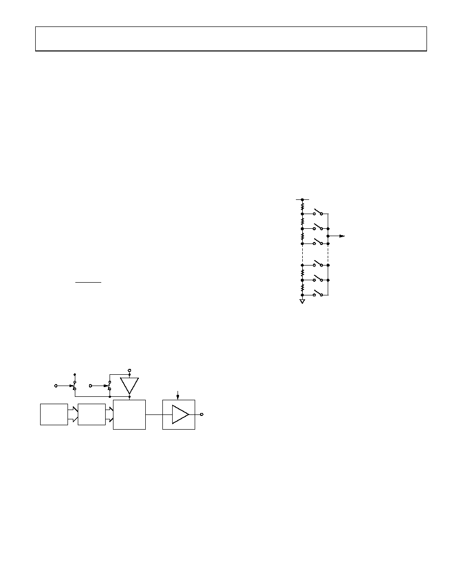
DIGITAL-TO-ANALOG CONVERTER
The architecture of one DAC channel consists of a resistor
string DAC followed by an output buffer amplifier. The voltage
at the VREF pin provides the reference voltage for the corre-
sponding DAC. Figure 29 shows a block diagram of the DAC
architecture. Since the input coding to the DAC is straight
binary, the ideal output voltage is given by
N
REF
OUT
D
V
2
×
=
where:
D
is the decimal equivalent of the binary code that is loaded to
the DAC register:
0 to 255 for AD5308 (8 bits)
0 to 1023 for AD5318 (10 bits)
0 to 4095 for AD5328 (12 bits)
N
is the DAC resolution.
INPUT
REGISTER
OUTPUT
BUFFER AMPLIFIER
REFERENCE
BUFFER
GAIN MODE
(GAIN = +1 OR +2)
VOUTA
VREFABCD
VDD
BUF
RESISTOR
STRING
DAC
REGISTER
02812
-029
VDD
Figure 29. Single DAC Channel Architecture
DAC Reference Inputs
There is a reference pin for each quad of DACs. The reference
inputs can be buffered from VDD, or unbuffered. The advantage
with the buffered input is the high impedance it presents to the
voltage source driving it. However, if the unbuffered mode is
used, the user can have a reference voltage as low as 0.25 V and
as high as VDD since there is no restriction due to the headroom
and footroom of the reference amplifier.
If there is a buffered reference in the circuit (for example, the
REF192), there is no need to use the on-chip buffers of the
AD5308/AD5318/AD5328. In unbuffered mode, the input
impedance is still large at typically 45 kΩ per reference input
for 0 V to VREF mode and 22 kΩ for 0 V to 2 VREF mode.
RESISTOR STRING
The resistor-string section is shown in Figure 30. It is simply a
string of resistors, each of value R. The digital code loaded to
the DAC register determines at which node on the string the
voltage is tapped off to be fed into the output amplifier. The
voltage is tapped off by closing one of the switches connecting
the string to the amplifier. Because it is a string of resistors, it is
guaranteed monotonic.
02812
-030
R
TO OUTPUT
AMPLIFIER
Figure 30. Resistor String
OUTPUT AMPLIFIER
The output buffer amplifier is capable of generating output
voltages to within 1 mV of either rail. Its actual range depends
on the value of VREF, the gain of the output amplifier, the offset
error, and the gain error.
If a gain of 1 is selected (gain bit = 0), the output range is
0.001 V to VREF.
If a gain of 2 is selected (gain bit = 1), the output range is
0.001 V to 2 VREF. Because of clamping, however, the maximum
output is limited to VDD 0.001 V.
The output amplifier is capable of driving a load of 2 kΩ to
GND or VDD, in parallel with 500 pF to GND or VDD. The
source and sink capabilities of the output amplifier can be seen
in the plot in Figure 14.
The slew rate is 0.7 V/μs with a half-scale settling time to
±0.5 LSB (at 8 bits) of 6 μs.
相关PDF资料 |
PDF描述 |
|---|---|
| VI-202-MY-F2 | CONVERTER MOD DC/DC 15V 50W |
| VE-BNX-MV-F4 | CONVERTER MOD DC/DC 5.2V 150W |
| AD7303BRZ | IC DAC 8BIT DUAL R-R 8-SOIC |
| VI-201-MY-F4 | CONVERTER MOD DC/DC 12V 50W |
| VE-BNX-MV-F3 | CONVERTER MOD DC/DC 5.2V 150W |
相关代理商/技术参数 |
参数描述 |
|---|---|
| AD5308ARUZ | 制造商:Analog Devices 功能描述:IC DAC 8BIT 167KSPS 16TSSOP |
| AD5308ARUZ-REEL7 | 功能描述:IC DAC 8BIT OCTAL W/BUFF 16TSSOP RoHS:是 类别:集成电路 (IC) >> 数据采集 - 数模转换器 系列:- 产品培训模块:Lead (SnPb) Finish for COTS Obsolescence Mitigation Program 标准包装:50 系列:- 设置时间:4µs 位数:12 数据接口:串行 转换器数目:2 电压电源:单电源 功率耗散(最大):- 工作温度:-40°C ~ 85°C 安装类型:表面贴装 封装/外壳:8-TSSOP,8-MSOP(0.118",3.00mm 宽) 供应商设备封装:8-uMAX 包装:管件 输出数目和类型:2 电压,单极 采样率(每秒):* 产品目录页面:1398 (CN2011-ZH PDF) |
| AD5308BRU | 功能描述:IC DAC 8BIT 2.5V OCTAL 16-TSSOP RoHS:否 类别:集成电路 (IC) >> 数据采集 - 数模转换器 系列:- 标准包装:47 系列:- 设置时间:2µs 位数:14 数据接口:并联 转换器数目:1 电压电源:单电源 功率耗散(最大):55µW 工作温度:-40°C ~ 85°C 安装类型:表面贴装 封装/外壳:28-SSOP(0.209",5.30mm 宽) 供应商设备封装:28-SSOP 包装:管件 输出数目和类型:1 电流,单极;1 电流,双极 采样率(每秒):* |
| AD5308BRU-REEL | 功能描述:IC DAC 8BIT OCTAL W/BUFF 16TSSOP RoHS:否 类别:集成电路 (IC) >> 数据采集 - 数模转换器 系列:- 标准包装:47 系列:- 设置时间:2µs 位数:14 数据接口:并联 转换器数目:1 电压电源:单电源 功率耗散(最大):55µW 工作温度:-40°C ~ 85°C 安装类型:表面贴装 封装/外壳:28-SSOP(0.209",5.30mm 宽) 供应商设备封装:28-SSOP 包装:管件 输出数目和类型:1 电流,单极;1 电流,双极 采样率(每秒):* |
| AD5308BRU-REEL7 | 功能描述:IC DAC 8BIT OCTAL W/BUFF 16TSSOP RoHS:否 类别:集成电路 (IC) >> 数据采集 - 数模转换器 系列:- 标准包装:47 系列:- 设置时间:2µs 位数:14 数据接口:并联 转换器数目:1 电压电源:单电源 功率耗散(最大):55µW 工作温度:-40°C ~ 85°C 安装类型:表面贴装 封装/外壳:28-SSOP(0.209",5.30mm 宽) 供应商设备封装:28-SSOP 包装:管件 输出数目和类型:1 电流,单极;1 电流,双极 采样率(每秒):* |
发布紧急采购,3分钟左右您将得到回复。