参数资料
| 型号: | AD5308ARUZ |
| 厂商: | Analog Devices Inc |
| 文件页数: | 9/28页 |
| 文件大小: | 0K |
| 描述: | IC DAC 8BIT OCTAL W/BUFF 16TSSOP |
| 产品培训模块: | Data Converter Fundamentals DAC Architectures |
| 标准包装: | 96 |
| 设置时间: | 6µs |
| 位数: | 8 |
| 数据接口: | DSP,MICROWIRE?,QSPI?,串行,SPI? |
| 转换器数目: | 8 |
| 电压电源: | 单电源 |
| 工作温度: | -40°C ~ 105°C |
| 安装类型: | 表面贴装 |
| 封装/外壳: | 16-TSSOP(0.173",4.40mm 宽) |
| 供应商设备封装: | 16-TSSOP |
| 包装: | 管件 |
| 输出数目和类型: | 8 电压,单极;8 电压,双极 |
| 采样率(每秒): | 167k |
| 产品目录页面: | 782 (CN2011-ZH PDF) |
第1页第2页第3页第4页第5页第6页第7页第8页当前第9页第10页第11页第12页第13页第14页第15页第16页第17页第18页第19页第20页第21页第22页第23页第24页第25页第26页第27页第28页
AD5308/AD5318/AD5328
Rev. F | Page 17 of 28
Control Functions
BUF
In the case of a control function, the MSB (Bit 15) is a 1. This is
followed by two control bits, which determine the mode. There
are four different control modes: reference and gain mode, LDAC
mode, power-down mode, and reset mode. The write sequences
for these modes are shown in
.
This controls whether the reference of a group of DACs is
buffered or unbuffered. The reference of the first group of DACs
(A, B, C, and D) is controlled by setting Bit 2, and the second
group of DACs (E, F, G, and H) is controlled by setting Bit 3.
0: unbuffered reference.
1: buffered reference.
Reference and Gain Mode
GAIN
This mode determines whether the reference for each group of
DACs is buffered, unbuffered, or from VDD. It also determines
the gain of the output amplifier. To set up the reference of both
groups, set the control bits to (00), set the GAIN bits, the BUF
bits, and the VDD bits.
The gain of the DACs is controlled by setting Bit 4 for the first
group of DACs (A, B, C, and D) and Bit 5 for the second group
of DACs (E, F, G, and H).
0: output range of 0 V to VREF.
1: output range of 0 V to 2 VREF.
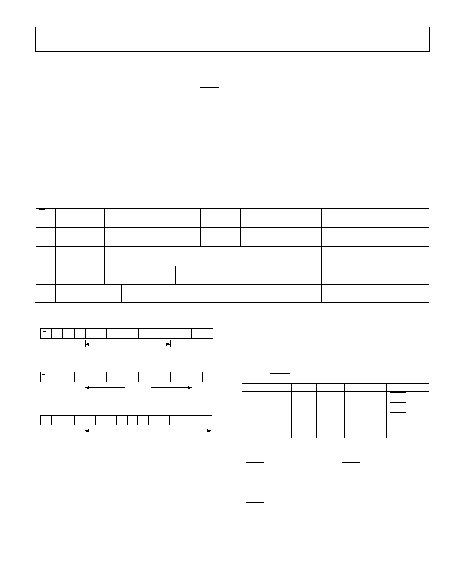
Table 7. Control Words for the AD53x8
D/C
Control Bits
15
14
13
12
11
10
9
8
7
6
5
4
3
2
1
0
Mode
GAIN Bits
BUF Bits
VDD Bits
Gain of output amplifier and
1
0
x
E...H
A...D
E...H
A...D
E...H
A...D
reference selection
LDAC Bits
LDAC
1
0
1
x
1/0
Channels
1
0
x
H
G
F
E
D
C
B
A
Power-down
Reset
1
1/0
x
Reset
LDAC Mode
02812-031
A0
D7
D6
D5
D4
D3
D2
D1
D0
0
BIT 0
(LSB)
BIT 15
(MSB)
DATA BITS
A1
A2
D/C
LDAC mode controls LDAC, which determines when data is
transferred from the input registers to the DAC registers. There
are three options when updating the DAC registers, as shown in
.
Figure 32. AD5308 Input Shift Register Contents
02812
-032
DATA BITS
A0
BIT 0
(LSB)
BIT 15
(MSB)
A1
D9
D8
D7
D6
D5
D4
D3
D2
D1
D0
0
A2
D/C
Table 8. LDAC Mode
Bit 15
Bit 14
Bit 13
Bits 12:2
Bit 1
Bit 0
Description
LDAC low
1
0
1
x ... x
0
Figure 33. AD5318 Input Shift Register Contents
LDAC high
1
0
1
x ... x
0
1
02812
-033
DATA BITS
A0
BIT 0
(LSB)
BIT 15
(MSB)
A1
A2
D9
D8
D7
D6
D5
D4
D3
D2
D1
D0
D10
D11
D/C
LDAC single
update
1
0
1
x ... x
1
0
1
0
1
x ... x
1
Reserved
Figure 34. AD5328 Input Shift Register Contents
LDAC Low (00): This option sets LDAC permanently low,
allowing the DAC registers to be updated continuously.
VDD
These bits are set when VDD is to be used as a reference. The
first group of DACs (A, B, C, and D) can be set up to use VDD by
setting Bit 0, and the second group of DACs (E, F, G, and H) by
setting Bit 1. The VDD bits have priority over the BUF bits.
LDAC High (01): This option sets LDAC permanently high.
The DAC registers are latched and the input registers can
change without affecting the contents of the DAC registers.
This is the default option for this mode.
When VDD is used as the reference, it is always unbuffered and
has an output range of 0 V to VREF regardless of the state of the
GAIN and BUF bits.
LDAC Single Update (10): This option causes a single pulse on
LDAC, updating the DAC registers once.
Reserved (11): reserved.
相关PDF资料 |
PDF描述 |
|---|---|
| VI-202-MY-F2 | CONVERTER MOD DC/DC 15V 50W |
| VE-BNX-MV-F4 | CONVERTER MOD DC/DC 5.2V 150W |
| AD7303BRZ | IC DAC 8BIT DUAL R-R 8-SOIC |
| VI-201-MY-F4 | CONVERTER MOD DC/DC 12V 50W |
| VE-BNX-MV-F3 | CONVERTER MOD DC/DC 5.2V 150W |
相关代理商/技术参数 |
参数描述 |
|---|---|
| AD5308ARUZ | 制造商:Analog Devices 功能描述:IC DAC 8BIT 167KSPS 16TSSOP |
| AD5308ARUZ-REEL7 | 功能描述:IC DAC 8BIT OCTAL W/BUFF 16TSSOP RoHS:是 类别:集成电路 (IC) >> 数据采集 - 数模转换器 系列:- 产品培训模块:Lead (SnPb) Finish for COTS Obsolescence Mitigation Program 标准包装:50 系列:- 设置时间:4µs 位数:12 数据接口:串行 转换器数目:2 电压电源:单电源 功率耗散(最大):- 工作温度:-40°C ~ 85°C 安装类型:表面贴装 封装/外壳:8-TSSOP,8-MSOP(0.118",3.00mm 宽) 供应商设备封装:8-uMAX 包装:管件 输出数目和类型:2 电压,单极 采样率(每秒):* 产品目录页面:1398 (CN2011-ZH PDF) |
| AD5308BRU | 功能描述:IC DAC 8BIT 2.5V OCTAL 16-TSSOP RoHS:否 类别:集成电路 (IC) >> 数据采集 - 数模转换器 系列:- 标准包装:47 系列:- 设置时间:2µs 位数:14 数据接口:并联 转换器数目:1 电压电源:单电源 功率耗散(最大):55µW 工作温度:-40°C ~ 85°C 安装类型:表面贴装 封装/外壳:28-SSOP(0.209",5.30mm 宽) 供应商设备封装:28-SSOP 包装:管件 输出数目和类型:1 电流,单极;1 电流,双极 采样率(每秒):* |
| AD5308BRU-REEL | 功能描述:IC DAC 8BIT OCTAL W/BUFF 16TSSOP RoHS:否 类别:集成电路 (IC) >> 数据采集 - 数模转换器 系列:- 标准包装:47 系列:- 设置时间:2µs 位数:14 数据接口:并联 转换器数目:1 电压电源:单电源 功率耗散(最大):55µW 工作温度:-40°C ~ 85°C 安装类型:表面贴装 封装/外壳:28-SSOP(0.209",5.30mm 宽) 供应商设备封装:28-SSOP 包装:管件 输出数目和类型:1 电流,单极;1 电流,双极 采样率(每秒):* |
| AD5308BRU-REEL7 | 功能描述:IC DAC 8BIT OCTAL W/BUFF 16TSSOP RoHS:否 类别:集成电路 (IC) >> 数据采集 - 数模转换器 系列:- 标准包装:47 系列:- 设置时间:2µs 位数:14 数据接口:并联 转换器数目:1 电压电源:单电源 功率耗散(最大):55µW 工作温度:-40°C ~ 85°C 安装类型:表面贴装 封装/外壳:28-SSOP(0.209",5.30mm 宽) 供应商设备封装:28-SSOP 包装:管件 输出数目和类型:1 电流,单极;1 电流,双极 采样率(每秒):* |
发布紧急采购,3分钟左右您将得到回复。