参数资料
| 型号: | AD5312BRMZ |
| 厂商: | Analog Devices Inc |
| 文件页数: | 13/24页 |
| 文件大小: | 0K |
| 描述: | IC DAC 10BIT DUAL R-R 10-MSOP |
| 产品培训模块: | Data Converter Fundamentals DAC Architectures |
| 标准包装: | 50 |
| 设置时间: | 6µs |
| 位数: | 10 |
| 数据接口: | 串行 |
| 转换器数目: | 2 |
| 电压电源: | 单电源 |
| 功率耗散(最大): | 2.5mW |
| 工作温度: | -40°C ~ 105°C |
| 安装类型: | 表面贴装 |
| 封装/外壳: | 10-TFSOP,10-MSOP(0.118",3.00mm 宽) |
| 供应商设备封装: | 10-MSOP |
| 包装: | 管件 |
| 输出数目和类型: | 2 电压,单极;2 电压,双极 |
| 采样率(每秒): | 143k |
| 产品目录页面: | 782 (CN2011-ZH PDF) |
AD5302/AD5312/AD5322
Rev. D | Page 20 of 24
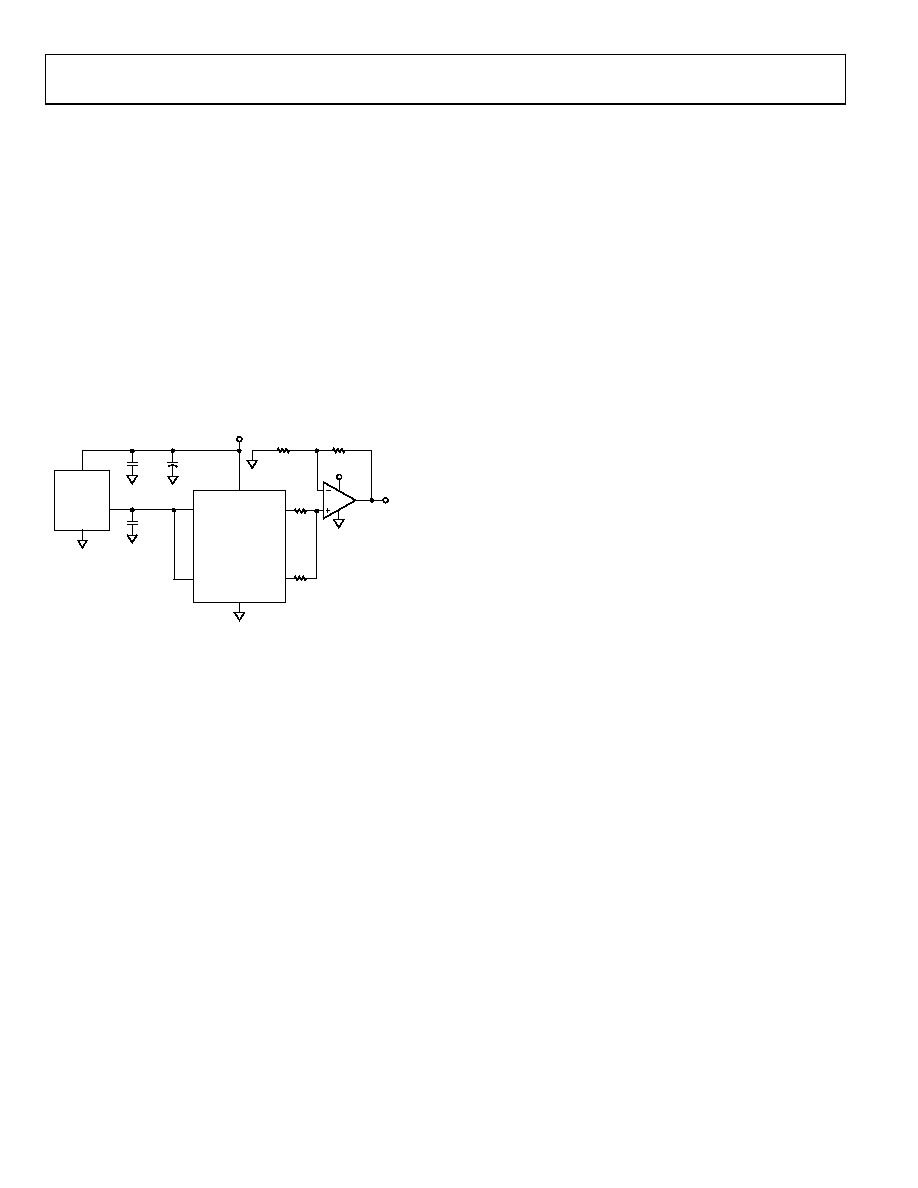
COARSE AND FINE ADJUSTMENT USING THE
AD5302/AD5312/AD5322
The DACs in the AD5302/AD5312/AD5322 can be paired
together to form a coarse and fine adjustment function, as
shown in Figure 44. DAC A is used to provide the coarse
adjustment while DAC B provides the fine adjustment. Varying
the ratio of R1 and R2 changes the relative effect of the coarse
and fine adjustments. With the resistor values and external
reference shown, the output amplifier has unity gain for the
DAC A output, so the output range is 0 V to 2.5 V 1 LSB. For
DAC B, the amplifier has a gain of 7.6 × 10⁻³, giving DAC B a
range equal to 19 mV.
The circuit is shown with a 2.5 V reference, but reference
voltages up to VDD can be used. The op amps indicated allow a
rail-to-rail output swing.
GND
AD5302/AD5312/
AD5322
EXT
REF
0
09
28-
0
44
VOUT
VOUTB
VREFA
1F
GND
VIN
0.1F
10F
VDD
VDD = 5V
+5V
AD820/
OP295
VOUTA
VREFB
R2
51.2k
R1
390
VOUT
R4
900
R3
51.2k
R2
51.2k
Figure 44. Coarse/Fine Adjustment
POWER SUPPLY BYPASSING AND GROUNDING
In any circuit where accuracy is important, careful considera-
tion of the power supply and ground return layout helps to
ensure the rated performance. The printed circuit board on
which the AD5302/AD5312/AD5322 is mounted should be
designed so that the analog and digital sections are separated
and confined to certain areas of the board. If the AD5302/
AD5312/AD5322 are in a system where multiple devices require
an AGND-to-DGND connection, the connection should be
made at one point only. The star ground point should be
established as close as possible to the AD5302/AD5312/
AD5322. The part should have ample supply bypassing of 10 μF
in parallel with 0.1 μF on the supply located as close as possible
to the package, ideally right up against the device. The 10 μF
capacitors are the tantalum bead type. The 0.1 μF capacitor
should have low effective series resistance (ESR) and effective
series inductance (ESI), similar to the common ceramic types
that provide a low impedance path to ground at high frequencies
that handle transient currents due to internal logic switching.
The power supply lines of the AD5302/AD5312/AD5322
should use as large a trace as possible to provide low impedance
paths and reduce the effects of glitches on the power supply line.
Fast switching signals such as clocks should be shielded with
digital ground to avoid radiating noise to other parts of the board,
and should never be run near the reference inputs. Avoid crossover
of digital and analog signals. Traces on opposite sides of the
board should run at right angles to each other. This reduces the
effects of feedthrough through the board. A microstrip technique
is by far the best, but is not always possible with a double-sided
board. In this technique, the component side of the board is dedi-
cated to ground while signal traces are placed on the solder side.
相关PDF资料 |
PDF描述 |
|---|---|
| VI-201-MY-F1 | CONVERTER MOD DC/DC 12V 50W |
| VI-J5R-MZ-F3 | CONVERTER MOD DC/DC 7.5V 25W |
| VI-J5R-MZ-F2 | CONVERTER MOD DC/DC 7.5V 25W |
| MS3454W14S-7P | CONN RCPT 3POS JAM NUT W/PINS |
| MS27472E22B2SD | CONN RCPT 85POS WALL MT W/SCKT |
相关代理商/技术参数 |
参数描述 |
|---|---|
| AD5312BRMZ-REEL | 功能描述:IC DAC 10BIT DUAL R-R 10-MSOP TR RoHS:是 类别:集成电路 (IC) >> 数据采集 - 数模转换器 系列:- 产品培训模块:LTC263x 12-, 10-, and 8-Bit VOUT DAC Family 特色产品:LTC2636 - Octal 12-/10-/8-Bit SPI VOUT DACs with 10ppm/°C Reference 标准包装:91 系列:- 设置时间:4µs 位数:10 数据接口:MICROWIRE?,串行,SPI? 转换器数目:8 电压电源:单电源 功率耗散(最大):2.7mW 工作温度:-40°C ~ 85°C 安装类型:表面贴装 封装/外壳:14-WFDFN 裸露焊盘 供应商设备封装:14-DFN-EP(4x3) 包装:管件 输出数目和类型:8 电压,单极 采样率(每秒):* |
| AD5312BRMZ-REEL7 | 功能描述:IC DAC 10BIT DUAL R-R 10-MSOP RoHS:是 类别:集成电路 (IC) >> 数据采集 - 数模转换器 系列:- 产品培训模块:LTC263x 12-, 10-, and 8-Bit VOUT DAC Family 特色产品:LTC2636 - Octal 12-/10-/8-Bit SPI VOUT DACs with 10ppm/°C Reference 标准包装:91 系列:- 设置时间:4µs 位数:10 数据接口:MICROWIRE?,串行,SPI? 转换器数目:8 电压电源:单电源 功率耗散(最大):2.7mW 工作温度:-40°C ~ 85°C 安装类型:表面贴装 封装/外壳:14-WFDFN 裸露焊盘 供应商设备封装:14-DFN-EP(4x3) 包装:管件 输出数目和类型:8 电压,单极 采样率(每秒):* |
| AD5312WARMZ-REEL7 | 制造商:Analog Devices 功能描述:AUTO VERSION! 2.5 V TO 5.5 V, 230 ?A, DUAL RAIL-TO-RAIL VOLT - Tape and Reel 制造商:Analog Devices 功能描述:ANAAD5312WARMZ-REEL7 DUAL 10-BIT VOLTAGE |
| AD5313 | 制造商:AD 制造商全称:Analog Devices 功能描述:2.5 V to 5.5 V, 500 uA, Parallel Interface Quad Voltage-Output 8-/10-/12-Bit DACs |
| AD5313ARU | 制造商:Analog Devices 功能描述:DAC 2-CH Resistor-String 10-bit 16-Pin TSSOP 制造商:Rochester Electronics LLC 功能描述:DUAL 10-BIT VOLTAGE OUT DAC I.C. - Bulk |
发布紧急采购,3分钟左右您将得到回复。