- 您现在的位置:买卖IC网 > PDF目录8716 > AD5313BRUZ-REEL7 (Analog Devices Inc)IC DAC 10BIT DUAL R-R 16-TSSOP PDF资料下载
参数资料
| 型号: | AD5313BRUZ-REEL7 |
| 厂商: | Analog Devices Inc |
| 文件页数: | 28/28页 |
| 文件大小: | 0K |
| 描述: | IC DAC 10BIT DUAL R-R 16-TSSOP |
| 产品培训模块: | Data Converter Fundamentals DAC Architectures |
| 标准包装: | 1,000 |
| 设置时间: | 7µs |
| 位数: | 10 |
| 数据接口: | 串行 |
| 转换器数目: | 2 |
| 电压电源: | 单电源 |
| 功率耗散(最大): | 2.5mW |
| 工作温度: | -40°C ~ 105°C |
| 安装类型: | 表面贴装 |
| 封装/外壳: | 16-TSSOP(0.173",4.40mm 宽) |
| 供应商设备封装: | 16-TSSOP |
| 包装: | 带卷 (TR) |
| 输出数目和类型: | 2 电压,单极;2 电压,双极 |
| 采样率(每秒): | 143k |
第1页第2页第3页第4页第5页第6页第7页第8页第9页第10页第11页第12页第13页第14页第15页第16页第17页第18页第19页第20页第21页第22页第23页第24页第25页第26页第27页当前第28页
AD5303/AD5313/AD5323
Rev. B | Page 9 of 28
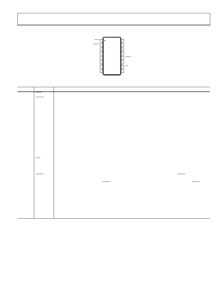
PIN CONFIGURATION AND FUNCTION DESCRIPTIONS
1
2
3
4
5
6
7
8
LDAC
VDD
VREFB
BUF A
VOUTA
VREFA
CLR
BUF B
16
15
14
13
12
11
10
9
GND
DIN
SCLK
PD
DCEN
VOUTB
SYNC
SDO
AD5303/
AD5313/
AD5323
TOP VIEW
(Not to Scale)
00
47
2-
00
4
Figure 6. Pin Configuration
Table 5. Pin Function Descriptions
Pin No.
Mnemonic
Description
1
CLR
Active Low Control Input. Loads all zeros to both input and DAC registers.
2
LDAC
Active Low Control Input. Transfers the contents of the input registers to their respective DAC registers. Pulsing
this pin low allows either or both DAC registers to be updated if the input registers have new data. This allows
the simultaneous update of both DAC outputs.
3
VDD
Power Supply Input. These parts can be operated from 2.5 V to 5.5 V, and the supply should be decoupled to GND.
4
VREFB
Reference Input Pin for DAC B. It may be configured as a buffered or an unbuffered input, depending on the state
of the BUF B pin. It has an input range from 0 V to VDD in unbuffered mode and from 1 V to VDD in buffered mode.
5
VREFA
Reference Input Pin for DAC A. It may be configured as a buffered or an unbuffered input depending on the state
of the BUF A pin. It has an input range from 0 to VDD in unbuffered mode and from 1 V to VDD in buffered mode.
6
VOUTA
Buffered Analog Output Voltage from DAC A. The output amplifier has rail-to-rail operation.
7
BUF A
Control Pin. Controls whether the reference input for DAC A is unbuffered or buffered. If this pin is tied low, the
reference input is unbuffered. If it is tied high, the reference input is buffered.
8
BUF B
Control Pin. Controls whether the reference input for DAC B is unbuffered or buffered. If this pin is tied low, the
reference input is unbuffered. If it is tied high, the reference input is buffered.
9
DCEN
This pin is used to enable the daisy-chaining option. This should be tied high if the part is being used in a daisy
chain. The pin should be tied low if it is being used in standalone mode.
10
PD
Active Low Control Input. Acts as a hardware power-down option. This pin overrides any software power-down
option. Both DACs go into power-down mode when this pin is tied low. The DAC outputs go into a high
impedance state and the current consumption of the part drops to 200 nA @ 5 V (50 nA @ 3 V).
11
VOUTB
Buffered Analog Output Voltage from DAC B. The output amplifier has rail-to-rail operation.
12
SYNC
Active Low Control Input. This is the frame synchronization signal for the input data. When SYNC goes low, it
powers on the SCLK and DIN buffers and enables the input shift register. Data is transferred in on the falling
edges of the following 16 clocks. If SYNC is taken high before the 16th falling edge, the rising edge of SYNC acts
as an interrupt and the write sequence is ignored by the device.
13
SCLK
Serial Clock Input. Data is clocked into the input shift register on the falling edge of the serial clock input. Data
can be transferred at rates up to 30 MHz. The SCLK input buffer is powered down after each write cycle.
14
DIN
Serial Data Input. This device has a 16-bit shift register. Data is clocked into the register on the falling edge of the
serial clock input. The DIN input buffer is powered down after each write cycle.
15
GND
Ground Reference Point for All Circuitry on the Part.
16
SDO
Serial Data Output. Can be used for daisy-chaining a number of these devices together or for reading back the
data in the shift register for diagnostic purposes. The serial data output is valid on the falling edge of the clock.
相关PDF资料 |
PDF描述 |
|---|---|
| VI-B1X-MV-F2 | CONVERTER MOD DC/DC 5.2V 150W |
| AD5662BRMZ-1REEL7 | IC DAC 16BIT BUFF V-OUT 8-MSOP |
| VE-2N4-MW-F4 | CONVERTER MOD DC/DC 48V 100W |
| VI-B1W-MV-F2 | CONVERTER MOD DC/DC 5.5V 150W |
| VI-B1T-MV-F2 | CONVERTER MOD DC/DC 6.5V 150W |
相关代理商/技术参数 |
参数描述 |
|---|---|
| AD5313R | 制造商:AD 制造商全称:Analog Devices 功能描述:Dual, 10-Bit nanoDAC with 2 ppm/C Reference, SPI Interface |
| AD5313RBCPZ-RL7 | 功能描述:数模转换器- DAC 10-Bit 2-CHSPI on-chip ref RoHS:否 制造商:Analog Devices 转换器数量:4 DAC 输出端数量:4 转换速率: 分辨率:12 bit 接口类型:Serial (I2C) 稳定时间: 最大工作温度:+ 105 C 安装风格: 封装 / 箱体:TSSOP 封装:Reel |
| AD5313RBRUZ | 功能描述:数模转换器- DAC 10-Bit 2-ch SPI nanoDAC+with on-chip ref RoHS:否 制造商:Texas Instruments 转换器数量:1 DAC 输出端数量:1 转换速率:2 MSPs 分辨率:16 bit 接口类型:QSPI, SPI, Serial (3-Wire, Microwire) 稳定时间:1 us 最大工作温度:+ 85 C 安装风格:SMD/SMT 封装 / 箱体:SOIC-14 封装:Tube |
| AD5313RBRUZ-RL7 | 功能描述:数模转换器- DAC 10-Bit 2-CHSPI on-chip ref RoHS:否 制造商:Analog Devices 转换器数量:4 DAC 输出端数量:4 转换速率: 分辨率:12 bit 接口类型:Serial (I2C) 稳定时间: 最大工作温度:+ 105 C 安装风格: 封装 / 箱体:TSSOP 封装:Reel |
| AD5313WBRUZ-REEL7 | 功能描述:IC DAC 10BIT DUAL R-R 16TSSOP RoHS:是 类别:集成电路 (IC) >> 数据采集 - 数模转换器 系列:- 产品培训模块:LTC263x 12-, 10-, and 8-Bit VOUT DAC Family 特色产品:LTC2636 - Octal 12-/10-/8-Bit SPI VOUT DACs with 10ppm/°C Reference 标准包装:91 系列:- 设置时间:4µs 位数:10 数据接口:MICROWIRE?,串行,SPI? 转换器数目:8 电压电源:单电源 功率耗散(最大):2.7mW 工作温度:-40°C ~ 85°C 安装类型:表面贴装 封装/外壳:14-WFDFN 裸露焊盘 供应商设备封装:14-DFN-EP(4x3) 包装:管件 输出数目和类型:8 电压,单极 采样率(每秒):* |
发布紧急采购,3分钟左右您将得到回复。