参数资料
| 型号: | AD5317BRU |
| 厂商: | Analog Devices Inc |
| 文件页数: | 11/28页 |
| 文件大小: | 0K |
| 描述: | IC DAC 10BIT QUAD W/BUFF 16TSSOP |
| 产品培训模块: | Data Converter Fundamentals DAC Architectures |
| 标准包装: | 96 |
| 设置时间: | 7µs |
| 位数: | 10 |
| 数据接口: | DSP,MICROWIRE?,QSPI?,串行,SPI? |
| 转换器数目: | 4 |
| 电压电源: | 单电源 |
| 工作温度: | -40°C ~ 105°C |
| 安装类型: | 表面贴装 |
| 封装/外壳: | 16-TSSOP(0.173",4.40mm 宽) |
| 供应商设备封装: | 16-TSSOP |
| 包装: | 管件 |
| 输出数目和类型: | 4 电压,单极;4 电压,双极 |
| 采样率(每秒): | 143k |
第1页第2页第3页第4页第5页第6页第7页第8页第9页第10页当前第11页第12页第13页第14页第15页第16页第17页第18页第19页第20页第21页第22页第23页第24页第25页第26页第27页第28页
AD5307/AD5317/AD5327
Rev. C | Page 19 of 28
The time to exit power-down is typically 2.5 μs for VDD = 5 V
and 5 μs when VDD = 3 V. This is the time from the rising edge
of PD to when the output voltage deviates from its power-down
voltage. See Figure 23 for a plot.
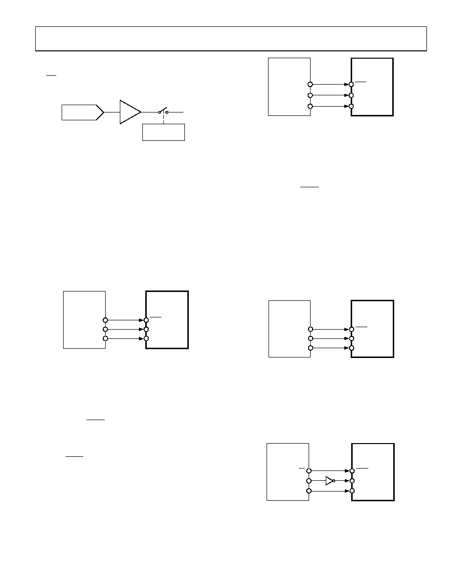
RESISTOR
STRING DAC
POWER-DOWN
CIRCUITRY
AMPLIFIER
VOUT
02067-036
Figure 36. Output Stage During Power-Down
MICROPROCESSOR INTERFACING
ADSP-2101/ADSP-2103-to-
AD5307/AD5317/AD5327 Interface
Figure 37 shows a serial interface between the AD5307/AD5317/
AD5327 and the ADSP-2101/ADSP-2103. The ADSP-2101/
ADSP-2103 should be set up to operate in the SPORT transmit
alternate framing mode. The ADSP-2101/ADSP-2103 SPORT is
programmed through the SPORT control register and should be
configured as follows: internal clock operation, active low framing,
16-bit word length. Transmission is initiated by writing a word
to the Tx register after SPORT is enabled. The data is clocked
out on each rising edge of the DSP’s serial clock and clocked
into the AD5307/AD5317/AD5327 on the falling edge of the
DAC’s SCLK.
SCLK
DIN
SYNC
TFS
DT
SCLK
ADSP-2101/
ADSP-21031
1ADDITIONAL PINS OMITTED FOR CLARITY.
02
06
7-
03
7
AD5307/
AD5317/
AD53271
Figure 37. ADSP-2101/ADSP-2103-to-AD5307/AD5317/AD5327 Interface
68HC11/68L11-to-AD5307/AD5317/AD5327 Interface
Figure 38 shows a serial interface between the AD5307/AD5317/
AD5327 and the 68HC11/68L11 microcontroller. SCK of the
68HC11/68L11 drives the SCLK of the AD5307/AD5317/
AD5327, and the MOSI output drives the serial data line (DIN)
of the DAC. The SYNC signal is derived from a port line (PC7).
The set-up conditions for correct operation of this interface are as
follows: The 68HC11/68L11 should be configured so that its CPOL
bit is 0 and its CPHA bit is 1. When data is being transmitted to the
DAC, the SYNC line is taken low (PC7). With this configuration,
data appearing on the MOSI output is valid on the falling edge
of SCK. Serial data from the 68HC11/68L11 is transmitted in
8-bit bytes, with only eight falling clock edges occurring in the
transmit cycle. Data is transmitted MSB first. To load data to
the AD5307/AD5317/AD5327, PC7 is left low after the first
eight bits are transferred and a second serial write operation
is performed to the DAC. PC7 is taken high at the end of this
procedure.
DIN
SCLK
SYNC
PC7
SCK
MOSI
68HC11/68L111
1ADDITIONAL PINS OMITTED FOR CLARITY.
0
2
0
6
7
-0
3
8
AD5307/
AD5317/
AD53271
Figure 38. 68HC11/68L11-to-AD5307/AD5317/AD5327 Interface
80C51/80L51-to-AD5307/AD5317/AD5327 Interface
Figure 39 shows a serial interface between the AD5307/AD5317/
AD5327 and the 80C51/80L51 microcontroller. The setup for
the interface is as follows: TxD of the 80C51/80L51 drives SCLK
of the AD5307/AD5317/AD5327, and RxD drives the serial data
line of the part. The SYNC signal is again derived from a bit-
programmable pin on the port. In this case, Port Line P3.3 is
used. When data is to be transmitted to the AD5307/AD5317/
AD5327, P3.3 is taken low. The 80C51/80L51 transmits data only
in 8-bit bytes; therefore, only eight falling clock edges occur in
the transmit cycle. To load data to the DAC, P3.3 is left low after
the first eight bits are transmitted, and a second write cycle is
initiated to transmit the second byte of data. P3.3 is taken high
following the completion of this cycle. The 80C51/80L51 outputs
the serial data LSB first. The AD5307/AD5317/AD5327 require
their data with the MSB as the first bit received. The
80C51/80L51 transmit routine should take this into account.
DIN
SCLK
P3.3
TxD
RxD
80C51/80L511
02
067
-03
9
SYNC
AD5307/
AD5317/
AD53271
1ADDITIONAL PINS OMITTED FOR CLARITY.
Figure 39. 80C51/80L51-to-AD5307/AD5317/AD5327 Interface
MICROWIRE-to-AD5307/AD5317/AD5327 Interface
Figure 40 shows an interface between the AD5307/AD5317/
AD5327 and a MICROWIRE-compatible device. Serial data is
shifted out on the falling edge of the serial clock, SK, and is
clocked into the AD5307/AD5317/AD5327 on the rising edge
of SK, which corresponds to the falling edge of the DAC’s SCLK.
DIN
SCLK
SK
SO
MICROWIRE1
1ADDITIONAL PINS OMITTED FOR CLARITY.
02
06
7-
04
0
CS
SYNC
AD5307/
AD5317/
AD53271
Figure 40. MICROWIRE-to-AD5307/AD5317/AD5327 Interface
相关PDF资料 |
PDF描述 |
|---|---|
| VE-25F-MW-B1 | CONVERTER MOD DC/DC 72V 100W |
| V375A3V3H264BL2 | CONVERTER MOD DC/DC 3.3V 264W |
| LTC2753IUK-12#TRPBF | IC DAC 12BIT DUAL 48-QFN |
| VI-J6M-MZ-B1 | CONVERTER MOD DC/DC 10V 25W |
| V375A3V3H264BF3 | CONVERTER MOD DC/DC 3.3V 264W |
相关代理商/技术参数 |
参数描述 |
|---|---|
| AD5317BRU-REEL | 功能描述:IC DAC 10BIT QUAD W/BUFF 16TSSOP RoHS:否 类别:集成电路 (IC) >> 数据采集 - 数模转换器 系列:- 标准包装:2,400 系列:- 设置时间:- 位数:18 数据接口:串行 转换器数目:3 电压电源:模拟和数字 功率耗散(最大):- 工作温度:-40°C ~ 85°C 安装类型:表面贴装 封装/外壳:36-TFBGA 供应商设备封装:36-TFBGA 包装:带卷 (TR) 输出数目和类型:* 采样率(每秒):* |
| AD5317BRU-REEL7 | 功能描述:IC DAC 10BIT QUAD W/BUFF 16TSSOP RoHS:否 类别:集成电路 (IC) >> 数据采集 - 数模转换器 系列:- 产品培训模块:LTC263x 12-, 10-, and 8-Bit VOUT DAC Family 特色产品:LTC2636 - Octal 12-/10-/8-Bit SPI VOUT DACs with 10ppm/°C Reference 标准包装:91 系列:- 设置时间:4µs 位数:10 数据接口:MICROWIRE?,串行,SPI? 转换器数目:8 电压电源:单电源 功率耗散(最大):2.7mW 工作温度:-40°C ~ 85°C 安装类型:表面贴装 封装/外壳:14-WFDFN 裸露焊盘 供应商设备封装:14-DFN-EP(4x3) 包装:管件 输出数目和类型:8 电压,单极 采样率(每秒):* |
| AD5317BRUZ | 功能描述:IC DAC 10BIT QUAD W/BUFF 16TSSOP RoHS:是 类别:集成电路 (IC) >> 数据采集 - 数模转换器 系列:- 产品培训模块:Lead (SnPb) Finish for COTS Obsolescence Mitigation Program 标准包装:50 系列:- 设置时间:4µs 位数:12 数据接口:串行 转换器数目:2 电压电源:单电源 功率耗散(最大):- 工作温度:-40°C ~ 85°C 安装类型:表面贴装 封装/外壳:8-TSSOP,8-MSOP(0.118",3.00mm 宽) 供应商设备封装:8-uMAX 包装:管件 输出数目和类型:2 电压,单极 采样率(每秒):* 产品目录页面:1398 (CN2011-ZH PDF) |
| AD5317BRUZ-REEL | 功能描述:IC DAC 10BIT QUAD W/BUFF 16TSSOP RoHS:是 类别:集成电路 (IC) >> 数据采集 - 数模转换器 系列:- 产品培训模块:LTC263x 12-, 10-, and 8-Bit VOUT DAC Family 特色产品:LTC2636 - Octal 12-/10-/8-Bit SPI VOUT DACs with 10ppm/°C Reference 标准包装:91 系列:- 设置时间:4µs 位数:10 数据接口:MICROWIRE?,串行,SPI? 转换器数目:8 电压电源:单电源 功率耗散(最大):2.7mW 工作温度:-40°C ~ 85°C 安装类型:表面贴装 封装/外壳:14-WFDFN 裸露焊盘 供应商设备封装:14-DFN-EP(4x3) 包装:管件 输出数目和类型:8 电压,单极 采样率(每秒):* |
| AD5317BRUZ-REEL7 | 功能描述:IC DAC 10BIT QUAD W/BUFF 16TSSOP RoHS:是 类别:集成电路 (IC) >> 数据采集 - 数模转换器 系列:- 产品培训模块:LTC263x 12-, 10-, and 8-Bit VOUT DAC Family 特色产品:LTC2636 - Octal 12-/10-/8-Bit SPI VOUT DACs with 10ppm/°C Reference 标准包装:91 系列:- 设置时间:4µs 位数:10 数据接口:MICROWIRE?,串行,SPI? 转换器数目:8 电压电源:单电源 功率耗散(最大):2.7mW 工作温度:-40°C ~ 85°C 安装类型:表面贴装 封装/外壳:14-WFDFN 裸露焊盘 供应商设备封装:14-DFN-EP(4x3) 包装:管件 输出数目和类型:8 电压,单极 采样率(每秒):* |
发布紧急采购,3分钟左右您将得到回复。