参数资料
| 型号: | AD5317BRU |
| 厂商: | Analog Devices Inc |
| 文件页数: | 14/28页 |
| 文件大小: | 0K |
| 描述: | IC DAC 10BIT QUAD W/BUFF 16TSSOP |
| 产品培训模块: | Data Converter Fundamentals DAC Architectures |
| 标准包装: | 96 |
| 设置时间: | 7µs |
| 位数: | 10 |
| 数据接口: | DSP,MICROWIRE?,QSPI?,串行,SPI? |
| 转换器数目: | 4 |
| 电压电源: | 单电源 |
| 工作温度: | -40°C ~ 105°C |
| 安装类型: | 表面贴装 |
| 封装/外壳: | 16-TSSOP(0.173",4.40mm 宽) |
| 供应商设备封装: | 16-TSSOP |
| 包装: | 管件 |
| 输出数目和类型: | 4 电压,单极;4 电压,双极 |
| 采样率(每秒): | 143k |
第1页第2页第3页第4页第5页第6页第7页第8页第9页第10页第11页第12页第13页当前第14页第15页第16页第17页第18页第19页第20页第21页第22页第23页第24页第25页第26页第27页第28页
AD5307/AD5317/AD5327
Rev. C | Page 21 of 28
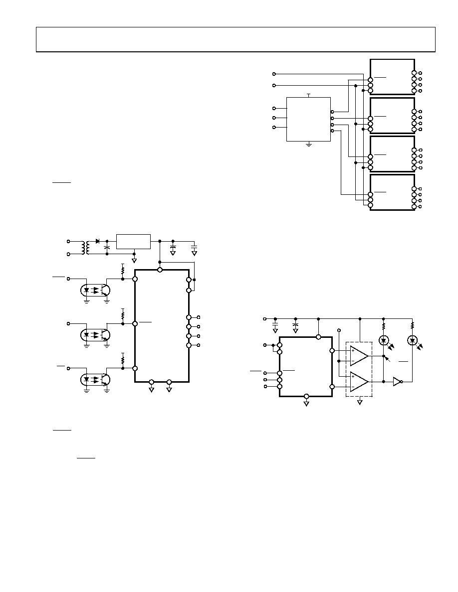
OPTO-ISOLATED INTERFACE FOR
PROCESS-CONTROL APPLICATIONS
The AD5307/AD5317/AD5327 each have a versatile 3-wire serial
interface, making them ideal for generating accurate voltages in
process-control and industrial applications. Due to noise, safety
requirements, or distance, it may be necessary to isolate the
AD5307/AD5317/AD5327 from the controller. This can easily
be achieved by using opto-isolators capable of providing isolation
in excess of 3 kV. The actual data rate achieved can be limited
by the type of optocouplers chosen. The serial loading structure
of the AD5307/AD5317/AD5327 makes them ideally suited for
use in opto-isolated applications. Figure 43 shows an opto-isolated
interface to the AD5307/AD5317/AD5327 where DIN, SCLK,
and SYNC are driven from optocouplers. The power supply to
the part should also be isolated. This is done by using a trans-
former. On the DAC side of the transformer, a 5 V regulator
provides the 5 V supply required for the AD5307/AD5317/
AD5327.
10k
DIN
GND
SCLK
5V
REGULATOR
POWER
10k
AD5307
DCEN
02
06
7-
0
43
SYNC
VOUTB
VOUTC
VOUTD
VREFAB
VREFCD
10F
0.1F
VOUTA
VDD
SCLK
DIN
SYNC
Figure 43. AD5307 in an Opto-Isolated Interface
DECODING MULTIPLE
AD5307/AD5317/AD5327 DEVICES
The SYNC pin on the AD5307/AD5317/AD5327 can be used in
applications to decode a number of DACs. In this application,
all DACs in the system receive the same serial clock and serial
data, but the SYNC to only one of the devices is active at any
given time, allowing access to four channels in this 16-channel
system. The 74HC139 is used as a 2-to-4 line decoder to address
any of the DACs in the system. To prevent timing errors, the
enable input should be brought to its inactive state while the
coded address inputs are changing state. Figure 44 shows a
diagram of a typical setup for decoding multiple AD5307
devices in a system.
74HC139
ENABLE
CODED
ADDRESS
1G
1A
1B
DGND
1Y0
1Y1
1Y2
1Y3
SCLK
DIN
SCLK
DIN
SCLK
DIN
SCLK
DIN
SCLK
AD5307
VOUTB
VOUTC
VOUTD
VOUTA
SYNC
VCC
VDD
VOUTB
VOUTC
VOUTD
VOUTA
VOUTB
VOUTC
VOUTD
VOUTA
VOUTB
VOUTC
VOUTD
VOUTA
02067-
044
SYNC
Figure 44. Decoding Multiple AD5307 Devices in a System
AD5307/AD5317/AD5327 AS DIGITALLY
PROGRAMMABLE WINDOW DETECTORS
A digitally programmable upper/lower limit detector using two of
the DACs in the AD5307/AD5317/AD5327 is shown in Figure 45.
The upper and lower limits for the test are loaded to DAC A
and DAC B, which, in turn, set the limits on the CMP04. If the
signal at the VIN input is not within the programmed window,
an LED indicates the fail condition. Similarly, DAC C and DAC D
can be used for window detection on a second VIN signal.
5V
SCLK
DIN
1/2
CMP04
1k
FAIL
1k
PASS
1/6 74HC05
SYNC
10F
0.1F
VREF
VIN
PASS/FAIL
AD5307/
AD5317/
AD5327
SCLK
DIN
GND
VOUTA
VREFAB
VREFCD
VOUTB
SYNC
VDD
020
67-
045
Figure 45. Window Detection
相关PDF资料 |
PDF描述 |
|---|---|
| VE-25F-MW-B1 | CONVERTER MOD DC/DC 72V 100W |
| V375A3V3H264BL2 | CONVERTER MOD DC/DC 3.3V 264W |
| LTC2753IUK-12#TRPBF | IC DAC 12BIT DUAL 48-QFN |
| VI-J6M-MZ-B1 | CONVERTER MOD DC/DC 10V 25W |
| V375A3V3H264BF3 | CONVERTER MOD DC/DC 3.3V 264W |
相关代理商/技术参数 |
参数描述 |
|---|---|
| AD5317BRU-REEL | 功能描述:IC DAC 10BIT QUAD W/BUFF 16TSSOP RoHS:否 类别:集成电路 (IC) >> 数据采集 - 数模转换器 系列:- 标准包装:2,400 系列:- 设置时间:- 位数:18 数据接口:串行 转换器数目:3 电压电源:模拟和数字 功率耗散(最大):- 工作温度:-40°C ~ 85°C 安装类型:表面贴装 封装/外壳:36-TFBGA 供应商设备封装:36-TFBGA 包装:带卷 (TR) 输出数目和类型:* 采样率(每秒):* |
| AD5317BRU-REEL7 | 功能描述:IC DAC 10BIT QUAD W/BUFF 16TSSOP RoHS:否 类别:集成电路 (IC) >> 数据采集 - 数模转换器 系列:- 产品培训模块:LTC263x 12-, 10-, and 8-Bit VOUT DAC Family 特色产品:LTC2636 - Octal 12-/10-/8-Bit SPI VOUT DACs with 10ppm/°C Reference 标准包装:91 系列:- 设置时间:4µs 位数:10 数据接口:MICROWIRE?,串行,SPI? 转换器数目:8 电压电源:单电源 功率耗散(最大):2.7mW 工作温度:-40°C ~ 85°C 安装类型:表面贴装 封装/外壳:14-WFDFN 裸露焊盘 供应商设备封装:14-DFN-EP(4x3) 包装:管件 输出数目和类型:8 电压,单极 采样率(每秒):* |
| AD5317BRUZ | 功能描述:IC DAC 10BIT QUAD W/BUFF 16TSSOP RoHS:是 类别:集成电路 (IC) >> 数据采集 - 数模转换器 系列:- 产品培训模块:Lead (SnPb) Finish for COTS Obsolescence Mitigation Program 标准包装:50 系列:- 设置时间:4µs 位数:12 数据接口:串行 转换器数目:2 电压电源:单电源 功率耗散(最大):- 工作温度:-40°C ~ 85°C 安装类型:表面贴装 封装/外壳:8-TSSOP,8-MSOP(0.118",3.00mm 宽) 供应商设备封装:8-uMAX 包装:管件 输出数目和类型:2 电压,单极 采样率(每秒):* 产品目录页面:1398 (CN2011-ZH PDF) |
| AD5317BRUZ-REEL | 功能描述:IC DAC 10BIT QUAD W/BUFF 16TSSOP RoHS:是 类别:集成电路 (IC) >> 数据采集 - 数模转换器 系列:- 产品培训模块:LTC263x 12-, 10-, and 8-Bit VOUT DAC Family 特色产品:LTC2636 - Octal 12-/10-/8-Bit SPI VOUT DACs with 10ppm/°C Reference 标准包装:91 系列:- 设置时间:4µs 位数:10 数据接口:MICROWIRE?,串行,SPI? 转换器数目:8 电压电源:单电源 功率耗散(最大):2.7mW 工作温度:-40°C ~ 85°C 安装类型:表面贴装 封装/外壳:14-WFDFN 裸露焊盘 供应商设备封装:14-DFN-EP(4x3) 包装:管件 输出数目和类型:8 电压,单极 采样率(每秒):* |
| AD5317BRUZ-REEL7 | 功能描述:IC DAC 10BIT QUAD W/BUFF 16TSSOP RoHS:是 类别:集成电路 (IC) >> 数据采集 - 数模转换器 系列:- 产品培训模块:LTC263x 12-, 10-, and 8-Bit VOUT DAC Family 特色产品:LTC2636 - Octal 12-/10-/8-Bit SPI VOUT DACs with 10ppm/°C Reference 标准包装:91 系列:- 设置时间:4µs 位数:10 数据接口:MICROWIRE?,串行,SPI? 转换器数目:8 电压电源:单电源 功率耗散(最大):2.7mW 工作温度:-40°C ~ 85°C 安装类型:表面贴装 封装/外壳:14-WFDFN 裸露焊盘 供应商设备封装:14-DFN-EP(4x3) 包装:管件 输出数目和类型:8 电压,单极 采样率(每秒):* |
发布紧急采购,3分钟左右您将得到回复。