参数资料
| 型号: | AD5320BRM |
| 厂商: | Analog Devices Inc |
| 文件页数: | 3/20页 |
| 文件大小: | 0K |
| 描述: | IC DAC 12BIT 2.7V R-R OUT 8-MSOP |
| 产品培训模块: | Data Converter Fundamentals DAC Architectures |
| 标准包装: | 50 |
| 设置时间: | 8µs |
| 位数: | 12 |
| 数据接口: | DSP,MICROWIRE?,QSPI?,串行,SPI? |
| 转换器数目: | 1 |
| 电压电源: | 单电源 |
| 工作温度: | -40°C ~ 105°C |
| 安装类型: | 表面贴装 |
| 封装/外壳: | 8-TSSOP,8-MSOP(0.118",3.00mm 宽) |
| 供应商设备封装: | 8-MSOP |
| 包装: | 管件 |
| 输出数目和类型: | 1 电压,双极 |
| 采样率(每秒): | 125k |
AD5320
Rev. C | Page 11 of 20
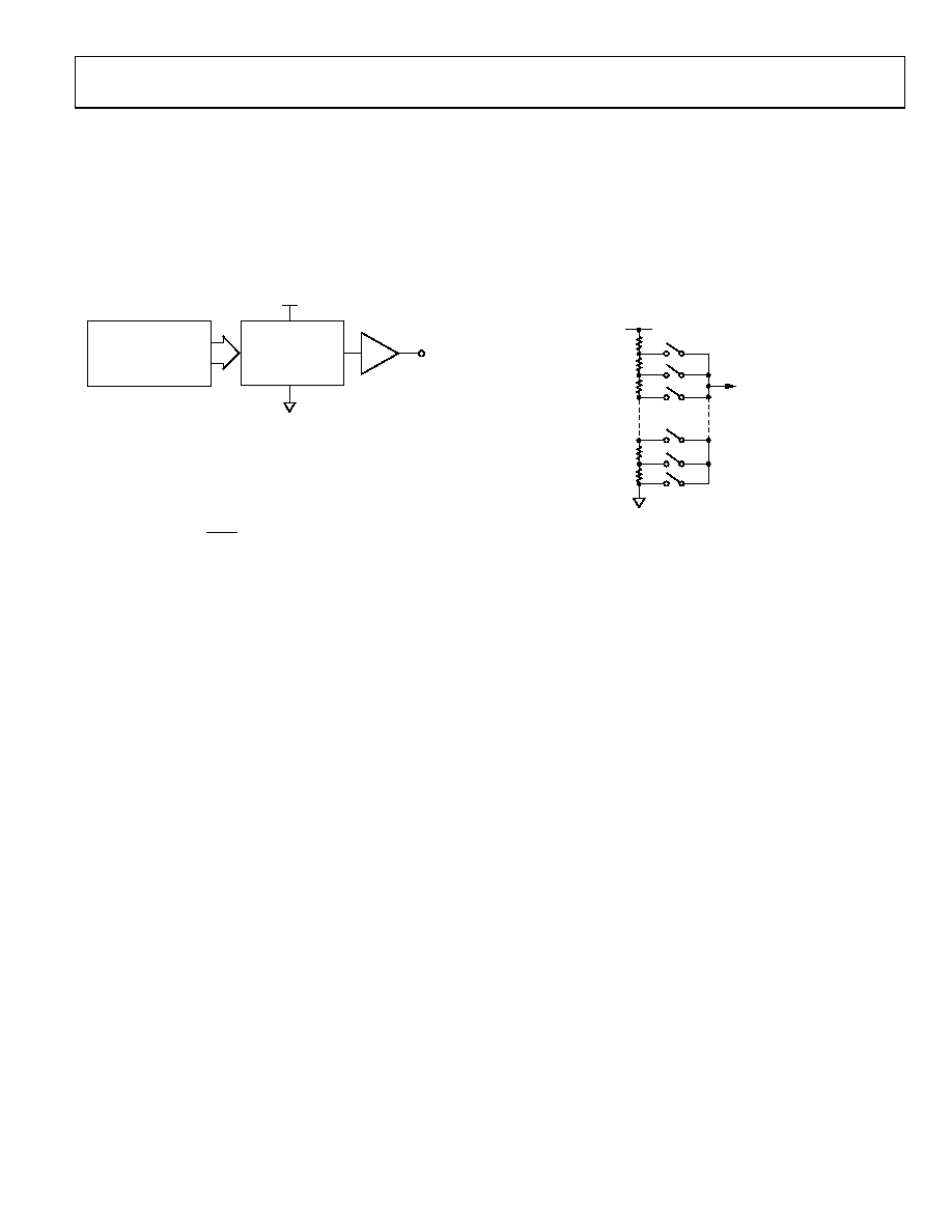
THEORY OF OPERATION
D/A SECTION
The AD5320 DAC is fabricated on a CMOS process. The
architecture consists of a string DAC followed by an output
buffer amplifier. Because there is no reference input pin, the
block diagram of the DAC architecture.
VDD
VOUT
GND
RESISTOR
STRING
REF (+)
REF (–)
OUTPUT
AMPLIFIER
DAC REGISTER
00
93
4-
0
23
Figure 23. DAC Architecture
Since the input coding to the DAC is straight binary, the ideal
output voltage is given by:
×
=
4096
D
V
DD
OUT
where D = decimal equivalent of the binary code that is loaded
to the DAC register; it can range from 0 to 4095.
RESISTOR STRING
The resistor string section is shown in Figure 24. It is simply a
string of resistors, each of value R. The code loaded to the DAC
register determines at which node on the string the voltage is
tapped off to be fed into the output amplifier. The voltage is
tapped off by closing one of the switches connecting the string
to the amplifier. Because it is a string of resistors, it is
guaranteed monotonic.
R
TO OUTPUT
AMPLIFIER
00
93
4-
0
24
Figure 24. Resistor String
OUTPUT AMPLIFIER
The output buffer amplifier is capable of generating rail-to-rail
voltages on its output that gives an output range of 0 V to VDD. It
is capable of driving a load of 2 kΩ in parallel with 1000 pF to
GND. The source and sink capabilities of the output amplifier
with a half-scale settling time of 8 μs with the output unloaded.
相关PDF资料 |
PDF描述 |
|---|---|
| AD5321BRM | IC DAC 12BIT 2.5V 2-WIRE 8-MSOP |
| AD5322BRM | IC DAC 12BIT DUAL R-R OUT 10MSOP |
| AD5323BRU | IC DAC 12 BIT DUAL R-R 16-TSSOP |
| AD5324BRM | IC DAC 12BIT QUAD 2.5V 10-MSOP |
| AD5325ARM | IC DAC 12BIT 2WIRE I2C 10-MSOP |
相关代理商/技术参数 |
参数描述 |
|---|---|
| AD5320BRM-REEL | 功能描述:IC DAC 12BIT R-R W/BUFF 8-MSOP RoHS:否 类别:集成电路 (IC) >> 数据采集 - 数模转换器 系列:- 标准包装:2,400 系列:- 设置时间:- 位数:18 数据接口:串行 转换器数目:3 电压电源:模拟和数字 功率耗散(最大):- 工作温度:-40°C ~ 85°C 安装类型:表面贴装 封装/外壳:36-TFBGA 供应商设备封装:36-TFBGA 包装:带卷 (TR) 输出数目和类型:* 采样率(每秒):* |
| AD5320BRM-REEL7 | 功能描述:IC DAC 12BIT R-R W/BUFF 8-MSOP RoHS:否 类别:集成电路 (IC) >> 数据采集 - 数模转换器 系列:- 标准包装:2,400 系列:- 设置时间:- 位数:18 数据接口:串行 转换器数目:3 电压电源:模拟和数字 功率耗散(最大):- 工作温度:-40°C ~ 85°C 安装类型:表面贴装 封装/外壳:36-TFBGA 供应商设备封装:36-TFBGA 包装:带卷 (TR) 输出数目和类型:* 采样率(每秒):* |
| AD5320BRMZ | 功能描述:IC DAC 12BIT R-R W/BUFF 8-MSOP RoHS:是 类别:集成电路 (IC) >> 数据采集 - 数模转换器 系列:- 产品培训模块:Lead (SnPb) Finish for COTS Obsolescence Mitigation Program 标准包装:50 系列:- 设置时间:4µs 位数:12 数据接口:串行 转换器数目:2 电压电源:单电源 功率耗散(最大):- 工作温度:-40°C ~ 85°C 安装类型:表面贴装 封装/外壳:8-TSSOP,8-MSOP(0.118",3.00mm 宽) 供应商设备封装:8-uMAX 包装:管件 输出数目和类型:2 电压,单极 采样率(每秒):* 产品目录页面:1398 (CN2011-ZH PDF) |
| AD5320BRMZ1 | 制造商:AD 制造商全称:Analog Devices 功能描述:2.7 V to 5.5 V, 140 ??A, Rail-to-Rail Output 12-Bit DAC in an SOT-23 |
| AD5320BRMZ-REEL | 功能描述:IC DAC 12BIT R-R W/BUFF 8-MSOP RoHS:是 类别:集成电路 (IC) >> 数据采集 - 数模转换器 系列:- 产品培训模块:LTC263x 12-, 10-, and 8-Bit VOUT DAC Family 特色产品:LTC2636 - Octal 12-/10-/8-Bit SPI VOUT DACs with 10ppm/°C Reference 标准包装:91 系列:- 设置时间:4µs 位数:10 数据接口:MICROWIRE?,串行,SPI? 转换器数目:8 电压电源:单电源 功率耗散(最大):2.7mW 工作温度:-40°C ~ 85°C 安装类型:表面贴装 封装/外壳:14-WFDFN 裸露焊盘 供应商设备封装:14-DFN-EP(4x3) 包装:管件 输出数目和类型:8 电压,单极 采样率(每秒):* |
发布紧急采购,3分钟左右您将得到回复。