参数资料
| 型号: | AD5320BRM |
| 厂商: | Analog Devices Inc |
| 文件页数: | 7/20页 |
| 文件大小: | 0K |
| 描述: | IC DAC 12BIT 2.7V R-R OUT 8-MSOP |
| 产品培训模块: | Data Converter Fundamentals DAC Architectures |
| 标准包装: | 50 |
| 设置时间: | 8µs |
| 位数: | 12 |
| 数据接口: | DSP,MICROWIRE?,QSPI?,串行,SPI? |
| 转换器数目: | 1 |
| 电压电源: | 单电源 |
| 工作温度: | -40°C ~ 105°C |
| 安装类型: | 表面贴装 |
| 封装/外壳: | 8-TSSOP,8-MSOP(0.118",3.00mm 宽) |
| 供应商设备封装: | 8-MSOP |
| 包装: | 管件 |
| 输出数目和类型: | 1 电压,双极 |
| 采样率(每秒): | 125k |
AD5320
Rev. C | Page 15 of 20
APPLICATIONS
USING REF19X AS A POWER SUPPLY FOR AD5320
Because the supply current required by the AD5320 is
extremely low, an alternative option is to use a REF19x voltage
required voltage to the part (see Figure 32). This is especially
useful if the power supply is noisy or if the system supply
voltages are at some value other than 5 V or 3 V (such as 15 V).
The REF19x outputs a steady supply voltage for the AD5320. If
the low dropout REF195 is used, the current it needs to supply
to the AD5320 is 140 μA. This is with no load on the output of
the DAC. When the DAC output is loaded, the REF195 also
needs to supply the current to the load. The total current
required (with a 5 kΩ load on the DAC output) is:
140 μA + (5 V/5 kΩ) = 1.14 mA
The load regulation of the REF195 is typically 2 ppm/mA,
which results in an error of 2.3 ppm (11.5 μV) for the 1.14 mA
current drawn from it. This corresponds to a 0.009 LSB error.
REF195
AD5320
DIN
SCLK
SYNC
15V
5V
140A
VOUT = 0V TO 5V
3-WIRE
SERIAL
INTERFACE
00
93
4-
03
2
Figure 32. REF195 as Power Supply to AD5320
BIPOLAR OPERATION USING THE AD5320
The AD5320 is designed for single-supply operation but a bipolar
output range is also possible using the circuit in Figure 33. The
circuit below gives an output voltage range of ±5 V. Rail-to-rail
operation at the amplifier output is achievable using an AD820 or
an OP295 as the output amplifier.
The output voltage for any input code can be calculated as
follows:
×
+
×
×
=
1
2
1
2
1
4096
R
V
R
D
V
DD
O
where D represents the input code in decimal (0 to 4095).
With VDD = 5 V, R1 = R2 = 10 kΩ:
V
D
V
O
5
4096
10
×
=
This is an output voltage range of ±5 V with 000 hex
corresponding to a 5 V output and FFF hex corresponding to
a +5 V output.
3-WIRE SERIAL INTERFACE
+5V
AD5320
10F
0.1F
VDD
VOUT
R1 = 10k
R2 = 10k
+5V
±5V
–5V
AD820/
OP295
00
934-
033
Figure 33. Bipolar Operation with the AD5320
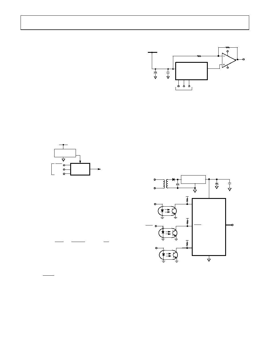
USING AD5320 WITH AN OPTO-ISOLATED
INTERFACE
For process control applications in industrial environments, it is
often necessary to use an opto-isolated interface to protect and
isolate the controlling circuitry from any hazardous common-
mode voltages that can occur in the area where the DAC is
functioning. Opto-isolators provide isolation in excess of 3 kV.
Because the AD5320 uses a 3-wire serial logic interface, it
requires only three opto-isolators to provide the required
isolation (see Figure 34). The power supply to the part also
needs to be isolated. This is done by using a transformer. On the
DAC side of the transformer, a 5 V regulator provides the 5 V
supply required for the AD5320.
VDD
0.1F
VDD
10k
VDD
10k
5V
REGULATOR
VOUT
GND
DIN
SYNC
SCLK
POWER
10F
VDD
SYNC
SCLK
DATA
AD5320
00
93
4-
0
34
Figure 34. AD5320 with An Opto-Isolated Interface
相关PDF资料 |
PDF描述 |
|---|---|
| AD5321BRM | IC DAC 12BIT 2.5V 2-WIRE 8-MSOP |
| AD5322BRM | IC DAC 12BIT DUAL R-R OUT 10MSOP |
| AD5323BRU | IC DAC 12 BIT DUAL R-R 16-TSSOP |
| AD5324BRM | IC DAC 12BIT QUAD 2.5V 10-MSOP |
| AD5325ARM | IC DAC 12BIT 2WIRE I2C 10-MSOP |
相关代理商/技术参数 |
参数描述 |
|---|---|
| AD5320BRM-REEL | 功能描述:IC DAC 12BIT R-R W/BUFF 8-MSOP RoHS:否 类别:集成电路 (IC) >> 数据采集 - 数模转换器 系列:- 标准包装:2,400 系列:- 设置时间:- 位数:18 数据接口:串行 转换器数目:3 电压电源:模拟和数字 功率耗散(最大):- 工作温度:-40°C ~ 85°C 安装类型:表面贴装 封装/外壳:36-TFBGA 供应商设备封装:36-TFBGA 包装:带卷 (TR) 输出数目和类型:* 采样率(每秒):* |
| AD5320BRM-REEL7 | 功能描述:IC DAC 12BIT R-R W/BUFF 8-MSOP RoHS:否 类别:集成电路 (IC) >> 数据采集 - 数模转换器 系列:- 标准包装:2,400 系列:- 设置时间:- 位数:18 数据接口:串行 转换器数目:3 电压电源:模拟和数字 功率耗散(最大):- 工作温度:-40°C ~ 85°C 安装类型:表面贴装 封装/外壳:36-TFBGA 供应商设备封装:36-TFBGA 包装:带卷 (TR) 输出数目和类型:* 采样率(每秒):* |
| AD5320BRMZ | 功能描述:IC DAC 12BIT R-R W/BUFF 8-MSOP RoHS:是 类别:集成电路 (IC) >> 数据采集 - 数模转换器 系列:- 产品培训模块:Lead (SnPb) Finish for COTS Obsolescence Mitigation Program 标准包装:50 系列:- 设置时间:4µs 位数:12 数据接口:串行 转换器数目:2 电压电源:单电源 功率耗散(最大):- 工作温度:-40°C ~ 85°C 安装类型:表面贴装 封装/外壳:8-TSSOP,8-MSOP(0.118",3.00mm 宽) 供应商设备封装:8-uMAX 包装:管件 输出数目和类型:2 电压,单极 采样率(每秒):* 产品目录页面:1398 (CN2011-ZH PDF) |
| AD5320BRMZ1 | 制造商:AD 制造商全称:Analog Devices 功能描述:2.7 V to 5.5 V, 140 ??A, Rail-to-Rail Output 12-Bit DAC in an SOT-23 |
| AD5320BRMZ-REEL | 功能描述:IC DAC 12BIT R-R W/BUFF 8-MSOP RoHS:是 类别:集成电路 (IC) >> 数据采集 - 数模转换器 系列:- 产品培训模块:LTC263x 12-, 10-, and 8-Bit VOUT DAC Family 特色产品:LTC2636 - Octal 12-/10-/8-Bit SPI VOUT DACs with 10ppm/°C Reference 标准包装:91 系列:- 设置时间:4µs 位数:10 数据接口:MICROWIRE?,串行,SPI? 转换器数目:8 电压电源:单电源 功率耗散(最大):2.7mW 工作温度:-40°C ~ 85°C 安装类型:表面贴装 封装/外壳:14-WFDFN 裸露焊盘 供应商设备封装:14-DFN-EP(4x3) 包装:管件 输出数目和类型:8 电压,单极 采样率(每秒):* |
发布紧急采购,3分钟左右您将得到回复。