- 您现在的位置:买卖IC网 > PDF目录8657 > AD5324ARM-REEL7 (Analog Devices Inc)IC DAC 12BIT QUAD VOUT 10MSOP TR PDF资料下载
参数资料
| 型号: | AD5324ARM-REEL7 |
| 厂商: | Analog Devices Inc |
| 文件页数: | 8/24页 |
| 文件大小: | 0K |
| 描述: | IC DAC 12BIT QUAD VOUT 10MSOP TR |
| 产品培训模块: | Data Converter Fundamentals DAC Architectures |
| 标准包装: | 1,000 |
| 设置时间: | 8µs |
| 位数: | 12 |
| 数据接口: | DSP,MICROWIRE?,QSPI?,串行,SPI? |
| 转换器数目: | 4 |
| 电压电源: | 单电源 |
| 工作温度: | -40°C ~ 105°C |
| 安装类型: | 表面贴装 |
| 封装/外壳: | 10-TFSOP,10-MSOP(0.118",3.00mm 宽) |
| 供应商设备封装: | 10-MSOP |
| 包装: | 带卷 (TR) |
| 输出数目和类型: | 4 电压,单极;4 电压,双极 |
| 采样率(每秒): | 125k |
AD5304/AD5314/AD5324
Data Sheet
Rev. H | Page 16 of 24
Double-Buffered Interface
The AD5304/AD5314/AD5324 DACs have double-buffered inter-
faces consisting of two banks of registers—input registers and
DAC registers. The input register is directly connected to the input
shift register and the digital code is transferred to the relevant input
register on completion of a valid write sequence. The DAC
register contains the digital code used by the resistor string.
Access to the DAC register is controlled by the LDAC bit. When
the LDAC bit is set high, the DAC register is latched and hence
the input register can change state without affecting the contents of
the DAC register. However, when the LDAC bit is set low, all DAC
registers are updated after a complete write sequence.
This is useful if the user requires simultaneous updating of all
DAC outputs. The user can write to three of the input registers
individually and then, by setting the LDAC bit low when
writing to the remaining DAC input register, all outputs
update simultaneously.
These parts contain an extra feature whereby the DAC register
is not updated unless its input register has been updated since
the last time that LDAC was brought low. Normally, when LDAC
is brought low, the DAC registers are filled with the contents of
the input registers. In the case of the AD5304/AD5314/AD5324,
the part updates the DAC register only if the input register has
been changed since the last time the DAC register was updated,
thereby removing unnecessary digital crosstalk.
POWER-DOWN MODE
The AD5304/AD5314/AD5324 have low power consumption,
dissipating only 1.5 mW with a 3 V supply and 3 mW with a
5 V supply. Power consumption can be further reduced when
the DACs are not in use by putting them into power-down mode,
selected by a 0 on Bit 13 (PD) of the control word.
When the PD bit is set to 1, all DACs work normally with a typical
power consumption of 600 μA at 5 V (500 μA at 3 V). However, in
power-down mode, the supply current falls to 200 nA at 5 V
(80 nA at 3 V) when all DACs are powered down. Not only does
the supply current drop, but also the output stage is internally
switched from the output of the amplifier, making it open-circuit.
This has the advantage that the output is three-stated while the
part is in power-down mode, and provides a defined input
condition for whatever is connected to the output of the DAC
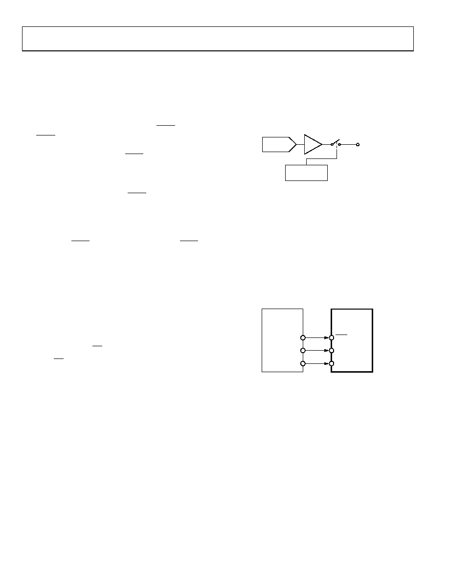
amplifier. The output stage is illustrated in Figure 35.
The bias generator, the output amplifier, the resistor string, and
all other associated linear circuitry are shut down when the power-
down mode is activated. However, the contents of the registers
are unaffected when in power-down. The time to exit power-down
is typically 2.5 μs for VDD = 5 V and 5 μs when VDD = 3 V. This is
the time from the falling edge of the 16th SCLK pulse to when
the output voltage deviates from its power down voltage. See
Figure 22 for a plot.
RESISTOR
STRING DAC
AMPLIFIER
VOUT
POWER-DOWN
CIRCUITRY
0
09
29
-0
35
Figure 35. Output Stage during Power-Down
MICROPROCESSOR INTERFACING
AD5304/AD5314/AD5324 to ADSP-21xx
Figure 36 shows a serial interface between the AD5304/AD5314/
AD5324 and the ADSP-21xx family. The ADSP-21xx is set up
to operate in the SPORT transmit alternate framing mode. The
ADSP-21xx sport is programmed through the SPORT control
register and must be configured as follows: internal clock operation,
active-low framing, and 16-bit word length. Transmission is
initiated by writing a word to the Tx register after the SPORT
has been enabled. The data is clocked out on each rising edge of
the DSP’s serial clock and clocked into the AD5304/AD5314/
AD5324 on the falling edge of the DAC’s SCLK.
AD5304/
AD5314/
AD5324*
ADSP-21xx*
*ADDITIONAL PINS OMITTED FOR CLARITY.
DIN
DT
SCLK
SYNC
TFS
0
09
29
-03
6
Figure 36. AD5304/AD5314/AD5324 to ADSP-21xx Interface
相关PDF资料 |
PDF描述 |
|---|---|
| LTC1448IS8#TR | IC DAC 12BIT DUAL R-R MPWR 8SOIC |
| LTC1588IG#TRPBF | IC DAC SOFTSPAN 12BIT 16-SSOP |
| CD4071BM | IC 2-INPUT OR GATE 14-SOIC |
| LTC1588IG#TR | IC DAC SOFTSPAN 12BIT 5V 16-SSOP |
| AD5541AACPZ-REEL7 | IC DAC 16BIT SERIAL IN 10MSOP |
相关代理商/技术参数 |
参数描述 |
|---|---|
| AD5324ARMZ | 功能描述:IC DAC 12BIT QUAD VOUT 10MSOP RoHS:是 类别:集成电路 (IC) >> 数据采集 - 数模转换器 系列:- 标准包装:1 系列:- 设置时间:4.5µs 位数:12 数据接口:串行,SPI? 转换器数目:1 电压电源:单电源 功率耗散(最大):- 工作温度:-40°C ~ 125°C 安装类型:表面贴装 封装/外壳:8-SOIC(0.154",3.90mm 宽) 供应商设备封装:8-SOICN 包装:剪切带 (CT) 输出数目和类型:1 电压,单极;1 电压,双极 采样率(每秒):* 其它名称:MCP4921T-E/SNCTMCP4921T-E/SNRCTMCP4921T-E/SNRCT-ND |
| AD5324ARMZ-REEL7 | 功能描述:IC DAC 12BIT QUAD VOUT 10-MSOP RoHS:是 类别:集成电路 (IC) >> 数据采集 - 数模转换器 系列:- 标准包装:47 系列:- 设置时间:2µs 位数:14 数据接口:并联 转换器数目:1 电压电源:单电源 功率耗散(最大):55µW 工作温度:-40°C ~ 85°C 安装类型:表面贴装 封装/外壳:28-SSOP(0.209",5.30mm 宽) 供应商设备封装:28-SSOP 包装:管件 输出数目和类型:1 电流,单极;1 电流,双极 采样率(每秒):* |
| AD5324BCPZ-REEL7 | 功能描述:IC DAC 12BIT QUAD VOUT 10LFCSP RoHS:是 类别:集成电路 (IC) >> 数据采集 - 数模转换器 系列:- 标准包装:47 系列:- 设置时间:2µs 位数:14 数据接口:并联 转换器数目:1 电压电源:单电源 功率耗散(最大):55µW 工作温度:-40°C ~ 85°C 安装类型:表面贴装 封装/外壳:28-SSOP(0.209",5.30mm 宽) 供应商设备封装:28-SSOP 包装:管件 输出数目和类型:1 电流,单极;1 电流,双极 采样率(每秒):* |
| AD5324BRM | 功能描述:IC DAC 12BIT QUAD 2.5V 10-MSOP RoHS:否 类别:集成电路 (IC) >> 数据采集 - 数模转换器 系列:- 产品培训模块:Data Converter Fundamentals DAC Architectures 标准包装:750 系列:- 设置时间:7µs 位数:16 数据接口:并联 转换器数目:1 电压电源:双 ± 功率耗散(最大):100mW 工作温度:0°C ~ 70°C 安装类型:表面贴装 封装/外壳:28-LCC(J 形引线) 供应商设备封装:28-PLCC(11.51x11.51) 包装:带卷 (TR) 输出数目和类型:1 电压,单极;1 电压,双极 采样率(每秒):143k |
| AD5324BRM-REEL | 功能描述:IC DAC 12BIT QUAD VOUT 10-MSOP RoHS:否 类别:集成电路 (IC) >> 数据采集 - 数模转换器 系列:- 标准包装:2,400 系列:- 设置时间:- 位数:18 数据接口:串行 转换器数目:3 电压电源:模拟和数字 功率耗散(最大):- 工作温度:-40°C ~ 85°C 安装类型:表面贴装 封装/外壳:36-TFBGA 供应商设备封装:36-TFBGA 包装:带卷 (TR) 输出数目和类型:* 采样率(每秒):* |
发布紧急采购,3分钟左右您将得到回复。