- 您现在的位置:买卖IC网 > PDF目录8657 > AD5324ARM-REEL7 (Analog Devices Inc)IC DAC 12BIT QUAD VOUT 10MSOP TR PDF资料下载
参数资料
| 型号: | AD5324ARM-REEL7 |
| 厂商: | Analog Devices Inc |
| 文件页数: | 9/24页 |
| 文件大小: | 0K |
| 描述: | IC DAC 12BIT QUAD VOUT 10MSOP TR |
| 产品培训模块: | Data Converter Fundamentals DAC Architectures |
| 标准包装: | 1,000 |
| 设置时间: | 8µs |
| 位数: | 12 |
| 数据接口: | DSP,MICROWIRE?,QSPI?,串行,SPI? |
| 转换器数目: | 4 |
| 电压电源: | 单电源 |
| 工作温度: | -40°C ~ 105°C |
| 安装类型: | 表面贴装 |
| 封装/外壳: | 10-TFSOP,10-MSOP(0.118",3.00mm 宽) |
| 供应商设备封装: | 10-MSOP |
| 包装: | 带卷 (TR) |
| 输出数目和类型: | 4 电压,单极;4 电压,双极 |
| 采样率(每秒): | 125k |
Data Sheet
AD5304/AD5314/AD5324
Rev. H | Page 17 of 24
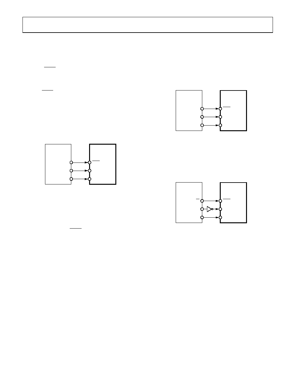
AD5304/AD5314/AD5324 to 68HC11/68L11 Interface
Figure 37 shows a serial interface between the AD5304/AD5314/
AD5324 and the 68HC11/68L11 microcontroller. SCK of the
68HC11/68L11 drives the SCLK of the AD5304/AD5314/AD5324,
while the MOSI output drives the serial data line (DIN) of the
DAC. The SYNC signal is derived from a port line (PC7). The
setup conditions for the correct operation of this interface are as
follows: the 68HC11/68L11 is configured so that its CPOL bit is
a 0 and its CPHA bit is a 1. When data is being transmitted to the
DAC, the SYNC line is taken low (PC7). When the 68HC11/68L11
is configured as above, data appearing on the MOSI output is
valid on the falling edge of SCK. Serial data from the 68HC11/
68L11 is transmitted in 8-bit bytes with only eight falling clock
edges occurring in the transmit cycle. Data is transmitted MSB
first. To load data to the AD5304/ AD5314/AD5324, PC7 is left
low after the first eight bits are transferred, a second serial write
operation is performed to the DAC, and PC7 is taken high at
the end of this procedure.
AD5304/
AD5314/
AD5324*
68HC11/68L11*
*ADDITIONAL PINS OMITTED FOR CLARITY.
SCLK
SCK
DIN
MOSI
SYNC
PC7
0
09
29
-03
7
Figure 37. AD5304/AD5314/AD5324 to 68HC11/68L11 Interface
AD5304/AD5314/AD5324 to 80C51/80L51 Interface
Figure 38 shows a serial interface between the AD5304/AD5314/
AD5324 and the 80C51/80L51 microcontroller. The setup for
the interface is as follows: TxD of the 80C51/80L51 drives SCLK
of the AD5304/AD5314/AD5324, while RxD drives the serial
data line of the part. The SYNC signal is again derived from a
bit-programmable pin on the port. In this case, port line P3.3 is
used. When data is to be transmitted to the AD5304/AD5314/
AD5324, P3.3 is taken low. The 80C51/80L51 transmits data
only in 8-bit bytes; thus only eight falling clock edges occur in
the transmit cycle. To load data to the DAC, P3.3 is left low after
the first eight bits are transmitted, and a second write cycle is
initiated to transmit the second byte of data. P3.3 is taken high
following the completion of this cycle. The 80C51/80L51 outputs
the serial data in a format that has the LSB first. The AD5304/
AD5314/AD5324 requires its data with the MSB as the first bit
received. The 80C51/80L51 transmit routine takes this into
account.
AD5304/
AD5314/
AD5324*
80C51/80L51*
*ADDITIONAL PINS OMITTED FOR CLARITY.
SCLK
TxD
DIN
RxD
SYNC
P3.3
0
09
29
-03
8
Figure 38. AD5304/AD5314/AD5324 to 80C51/80L51 Interface
AD5304/AD5314/AD5324 to MICROWIRE Interface
Figure 39 shows an interface between the AD5304/AD5314/
AD5324 and any MICROWIRE-compatible device. Serial data
is shifted out on the falling edge of the serial clock, SK, and is
clocked into the AD5304/AD5314/AD5324 on the rising edge
of SK, which corresponds to the falling edge of the DAC’s SCLK.
AD5304/
AD5314/
AD5324*
MICROWIRE*
*ADDITIONAL PINS OMITTED FOR CLARITY.
SCLK
SK
DIN
SO
SYNC
CS
0
09
29
-03
9
Figure 39. AD5304/AD5314/AD5324 to MICROWIRE Interface
相关PDF资料 |
PDF描述 |
|---|---|
| LTC1448IS8#TR | IC DAC 12BIT DUAL R-R MPWR 8SOIC |
| LTC1588IG#TRPBF | IC DAC SOFTSPAN 12BIT 16-SSOP |
| CD4071BM | IC 2-INPUT OR GATE 14-SOIC |
| LTC1588IG#TR | IC DAC SOFTSPAN 12BIT 5V 16-SSOP |
| AD5541AACPZ-REEL7 | IC DAC 16BIT SERIAL IN 10MSOP |
相关代理商/技术参数 |
参数描述 |
|---|---|
| AD5324ARMZ | 功能描述:IC DAC 12BIT QUAD VOUT 10MSOP RoHS:是 类别:集成电路 (IC) >> 数据采集 - 数模转换器 系列:- 标准包装:1 系列:- 设置时间:4.5µs 位数:12 数据接口:串行,SPI? 转换器数目:1 电压电源:单电源 功率耗散(最大):- 工作温度:-40°C ~ 125°C 安装类型:表面贴装 封装/外壳:8-SOIC(0.154",3.90mm 宽) 供应商设备封装:8-SOICN 包装:剪切带 (CT) 输出数目和类型:1 电压,单极;1 电压,双极 采样率(每秒):* 其它名称:MCP4921T-E/SNCTMCP4921T-E/SNRCTMCP4921T-E/SNRCT-ND |
| AD5324ARMZ-REEL7 | 功能描述:IC DAC 12BIT QUAD VOUT 10-MSOP RoHS:是 类别:集成电路 (IC) >> 数据采集 - 数模转换器 系列:- 标准包装:47 系列:- 设置时间:2µs 位数:14 数据接口:并联 转换器数目:1 电压电源:单电源 功率耗散(最大):55µW 工作温度:-40°C ~ 85°C 安装类型:表面贴装 封装/外壳:28-SSOP(0.209",5.30mm 宽) 供应商设备封装:28-SSOP 包装:管件 输出数目和类型:1 电流,单极;1 电流,双极 采样率(每秒):* |
| AD5324BCPZ-REEL7 | 功能描述:IC DAC 12BIT QUAD VOUT 10LFCSP RoHS:是 类别:集成电路 (IC) >> 数据采集 - 数模转换器 系列:- 标准包装:47 系列:- 设置时间:2µs 位数:14 数据接口:并联 转换器数目:1 电压电源:单电源 功率耗散(最大):55µW 工作温度:-40°C ~ 85°C 安装类型:表面贴装 封装/外壳:28-SSOP(0.209",5.30mm 宽) 供应商设备封装:28-SSOP 包装:管件 输出数目和类型:1 电流,单极;1 电流,双极 采样率(每秒):* |
| AD5324BRM | 功能描述:IC DAC 12BIT QUAD 2.5V 10-MSOP RoHS:否 类别:集成电路 (IC) >> 数据采集 - 数模转换器 系列:- 产品培训模块:Data Converter Fundamentals DAC Architectures 标准包装:750 系列:- 设置时间:7µs 位数:16 数据接口:并联 转换器数目:1 电压电源:双 ± 功率耗散(最大):100mW 工作温度:0°C ~ 70°C 安装类型:表面贴装 封装/外壳:28-LCC(J 形引线) 供应商设备封装:28-PLCC(11.51x11.51) 包装:带卷 (TR) 输出数目和类型:1 电压,单极;1 电压,双极 采样率(每秒):143k |
| AD5324BRM-REEL | 功能描述:IC DAC 12BIT QUAD VOUT 10-MSOP RoHS:否 类别:集成电路 (IC) >> 数据采集 - 数模转换器 系列:- 标准包装:2,400 系列:- 设置时间:- 位数:18 数据接口:串行 转换器数目:3 电压电源:模拟和数字 功率耗散(最大):- 工作温度:-40°C ~ 85°C 安装类型:表面贴装 封装/外壳:36-TFBGA 供应商设备封装:36-TFBGA 包装:带卷 (TR) 输出数目和类型:* 采样率(每秒):* |
发布紧急采购,3分钟左右您将得到回复。