参数资料
| 型号: | AD5326BRU |
| 厂商: | Analog Devices Inc |
| 文件页数: | 23/24页 |
| 文件大小: | 0K |
| 描述: | IC DAC 12BIT QUAD W/BUFF 16TSSOP |
| 产品培训模块: | Data Converter Fundamentals DAC Architectures |
| 标准包装: | 1 |
| 设置时间: | 8µs |
| 位数: | 12 |
| 数据接口: | I²C,串行 |
| 转换器数目: | 4 |
| 电压电源: | 单电源 |
| 功率耗散(最大): | 4.5mW |
| 工作温度: | -40°C ~ 105°C |
| 安装类型: | 表面贴装 |
| 封装/外壳: | 16-TSSOP(0.173",4.40mm 宽) |
| 供应商设备封装: | 16-TSSOP |
| 包装: | 管件 |
| 输出数目和类型: | 4 电压,单极;4 电压,双极 |
| 采样率(每秒): | 125k |
AD5306/AD5316/AD5326
Rev. F | Page 8 of 24
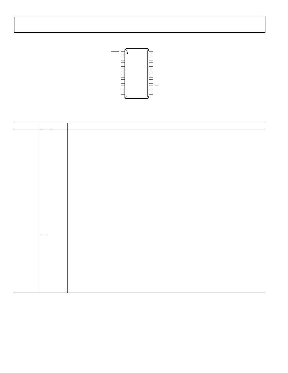
PIN CONFIGURATION AND FUNCTION DESCRIPTIONS
1
2
3
4
5
6
7
8
16
15
14
13
12
11
10
9
VDD
VOUTA
VOUTB
VREFB
VREFA
VOUTC
LDAC
A0
SCL
SDA
PD
VREFCVREFD
VOUTD
GND
A1
AD5306/
AD5316/
AD5326
TOP VIEW
(Not to Scale)
02066-003
Figure 3. Pin Configuration
Table 5. Pin Function Descriptions
Pin No.
Mnemonic
Description
1
LDAC
Active Low Control Input. Transfers the contents of the input registers to their respective DAC registers.
Pulsing this pin low allows any or all DAC registers to be updated if the input registers have new data. This
allows simultaneous update of all DAC outputs. Alternatively, this pin can be tied permanently low.
2
VDD
Power Supply Input. These parts can be operated from 2.5 V to 5.5 V and the supply should be decoupled
with a10 μF capacitor in parallel with a 0.1 μF capacitor to GND.
3
VOUTA
Buffered Analog Output Voltage from DAC A. The output amplifier has rail-to-rail operation.
4
VOUTB
Buffered Analog Output Voltage from DAC B. The output amplifier has rail-to-rail operation.
5
VOUTC
Buffered Analog Output Voltage from DAC C. The output amplifier has rail-to-rail operation.
6
VREFA
Reference Input Pin for DAC A. This pin can be configured as a buffered or an unbuffered input depending on
the state of the BUF bit in the input word to DAC A. It has an input range from 0.25 V to VDD in unbuffered
mode and from 1 V to VDD in buffered mode.
7
VREFB
Reference Input Pin for DAC B. This pin can be configured as a buffered or an unbuffered input depending on
the state of the BUF bit in the input word to DAC B. It has an input range from 0.25 V to VDD in unbuffered
mode and from 1 V to VDD in buffered mode.
8
VREFC
Reference Input Pin for DAC C. This pin can be configured as a buffered or an unbuffered input depending on
the state of the BUF bit in the input word to DAC C. It has an input range from 0.25 V to VDD in unbuffered
mode and from 1 V to VDD in buffered mode.
9
VREFD
Reference Input Pin for DAC D. This pin can be configured as a buffered or an unbuffered input depending on
the state of the BUF bit in the input word to DAC D. It has an input range from 0.25 V to VDD in unbuffered
mode and from 1 V to VDD in buffered mode.
10
PD
Active Low Control Input. Acts as a hardware power-down option. All DACs go into power-down mode when
this pin is tied low. The DAC outputs go into a high impedance state. The current consumption of the part
drops to 300 nA @ 5 V (90 nA @ 3 V).
11
VOUTD
Buffered Analog Output Voltage from DAC D. The output amplifier has rail-to-rail operation.
12
GND
Ground Reference Point for All Circuitry on the Part.
13
SDA
Serial Data Line. This is used in conjunction with the SCL line to clock data into the 16-bit input shift register.
It is a bidirectional open-drain data line that should be pulled to the supply with an external pull-up resistor.
14
SCL
Serial Clock Line. This is used in conjunction with the SDA line to clock data into the 16-bit input shift register.
Clock rates of up to 400 kbps can be accommodated in the I2C-compatible interface.
15
A0
Address Input. Sets the LSB of the 7-bit slave address.
16
A1
Address Input. Sets the second LSB of the 7-bit slave address.
相关PDF资料 |
PDF描述 |
|---|---|
| AD5327BRU | IC DAC 12BIT QUAD 2.5V 16-TSSOP |
| AD5328BRU | IC DAC 12BIT 2.5V OCTAL 16-TSSOP |
| AD53508JP | IC DUAL PARAMETRIC MEASURE44PLCC |
| AD5371BSTZ | IC DAC 14BIT 40CH SER 80-LQFP |
| AD5383BSTZ-5 | IC DAC 12BIT 32CH 5V 100-LQFP |
相关代理商/技术参数 |
参数描述 |
|---|---|
| AD5326BRU-REEL | 制造商:Analog Devices 功能描述:DAC 4-CH Resistor-String 12-bit 16-Pin TSSOP T/R 制造商:Analog Devices 功能描述:DAC 4-CH RES-STRING 12-BIT 16TSSOP - Tape and Reel |
| AD5326BRU-REEL7 | 功能描述:IC DAC 12BIT QUAD W/BUFF 16TSSOP RoHS:否 类别:集成电路 (IC) >> 数据采集 - 数模转换器 系列:- 标准包装:2,400 系列:- 设置时间:- 位数:18 数据接口:串行 转换器数目:3 电压电源:模拟和数字 功率耗散(最大):- 工作温度:-40°C ~ 85°C 安装类型:表面贴装 封装/外壳:36-TFBGA 供应商设备封装:36-TFBGA 包装:带卷 (TR) 输出数目和类型:* 采样率(每秒):* |
| AD5326BRUZ | 功能描述:IC DAC 12BIT QUAD W/BUFF 16TSSOP RoHS:是 类别:集成电路 (IC) >> 数据采集 - 数模转换器 系列:- 产品培训模块:Lead (SnPb) Finish for COTS Obsolescence Mitigation Program 标准包装:50 系列:- 设置时间:4µs 位数:12 数据接口:串行 转换器数目:2 电压电源:单电源 功率耗散(最大):- 工作温度:-40°C ~ 85°C 安装类型:表面贴装 封装/外壳:8-TSSOP,8-MSOP(0.118",3.00mm 宽) 供应商设备封装:8-uMAX 包装:管件 输出数目和类型:2 电压,单极 采样率(每秒):* 产品目录页面:1398 (CN2011-ZH PDF) |
| AD5326BRUZ1 | 制造商:AD 制造商全称:Analog Devices 功能描述:2.5 V to 5.5 V, 400 ??A, 2-Wire Interface, Quad Voltage Output, 8-/10-/12-Bit DACs |
| AD5326BRUZ-REEL | 功能描述:IC DAC 12BIT QUAD W/BUFF 16TSSOP RoHS:是 类别:集成电路 (IC) >> 数据采集 - 数模转换器 系列:- 标准包装:47 系列:- 设置时间:2µs 位数:14 数据接口:并联 转换器数目:1 电压电源:单电源 功率耗散(最大):55µW 工作温度:-40°C ~ 85°C 安装类型:表面贴装 封装/外壳:28-SSOP(0.209",5.30mm 宽) 供应商设备封装:28-SSOP 包装:管件 输出数目和类型:1 电流,单极;1 电流,双极 采样率(每秒):* |
发布紧急采购,3分钟左右您将得到回复。