参数资料
| 型号: | AD5331BRUZ |
| 厂商: | Analog Devices Inc |
| 文件页数: | 14/28页 |
| 文件大小: | 0K |
| 描述: | IC DAC 10BIT SNGL VOUT 20TSSOP |
| 产品培训模块: | Data Converter Fundamentals DAC Architectures |
| 标准包装: | 75 |
| 设置时间: | 7µs |
| 位数: | 10 |
| 数据接口: | 并联 |
| 转换器数目: | 1 |
| 电压电源: | 单电源 |
| 功率耗散(最大): | 1.25mW |
| 工作温度: | -40°C ~ 105°C |
| 安装类型: | 表面贴装 |
| 封装/外壳: | 20-TSSOP(0.173",4.40mm 宽) |
| 供应商设备封装: | 20-TSSOP |
| 包装: | 管件 |
| 输出数目和类型: | 1 电压,单极;1 电压,双极 |
| 采样率(每秒): | 143k |
| 产品目录页面: | 782 (CN2011-ZH PDF) |
第1页第2页第3页第4页第5页第6页第7页第8页第9页第10页第11页第12页第13页当前第14页第15页第16页第17页第18页第19页第20页第21页第22页第23页第24页第25页第26页第27页第28页
AD5330/AD5331/AD5340/AD5341
Rev. A | Page 21 of 28
APPLICATIONS INFORMATION
TYPICAL APPLICATION CIRCUITS
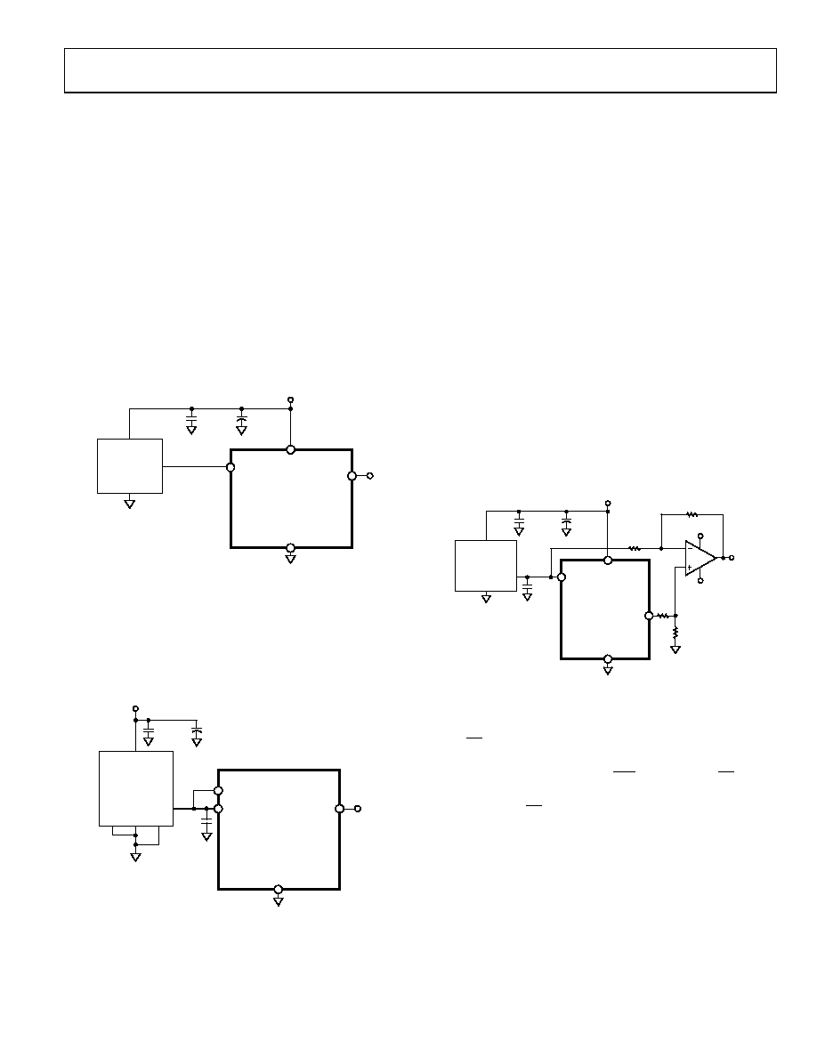
The AD5330/AD5331/AD5340/AD5341 can be used with
a wide range of reference voltages, especially if the reference
inputs are configured to be unbuffered, in which case the
devices offer full, one-quadrant multiplying capability over a
reference range of 0.25 V to VDD. More typically, these devices
can be used with a fixed, precision reference voltage. Figure 43
shows a typical setup for the devices when using an external
reference connected to the unbuffered reference inputs. If the
reference inputs are unbuffered, the reference input range is
from 0.25 V to VDD, but if the on-chip reference buffers are
used, the reference range is reduced. Suitable references for 5 V
suitable external reference is the AD589, a 1.23 V band gap
reference.
AD5330/AD5331/
AD5340/AD5341
VOUT
VDD = 2.5V TO 5.5V
VDD
GND
VREF
GND
EXT
REF
+
0.1F
10F
VOUT
VIN
AD780/REF192
WITH VDD = 5V
OR
AD589 WITH VDD = 2.5V
06
85
2-
044
Figure 43. AD5330/AD5331/AD5340/AD5341 Using External Reference
DRIVING VDD FROM THE REFERENCE VOLTAGE
If an output range of 0 V to VDD is required, the simplest
solution is to connect the reference inputs to VDD. Because this
supply may not be very accurate and may be noisy, the devices
can be powered from the reference voltage, for example using
a 5 V reference such as the ADP667, as shown in Figure 44.
AD5330/AD5331/
AD5340/AD5341
GND SHDN
VOUT
ADP667
VSET
6V TO 16V
VOUT
VDD
VIN
GND
VREF
+
0.1F
10F
06
85
2-
0
45
Figure 44. Using an ADP667 as Power and Reference to
AD5330/AD5331/AD5340/AD5341
BIPOLAR OPERATION USING THE AD5330/AD5331/
AD5340/AD5341
The AD5330/AD5331/AD5340/AD5341 are designed for
single-supply operation, but bipolar operation is achievable
using the circuit shown in Figure 45. The circuit shown has
been configured to achieve an output voltage range of –5 V <
VO < +5 V. Rail-to-rail operation at the amplifier output is
The output voltage for any input code can be calculated as follows:
VO
= [(1 + R4/R3) × (R2/(R1 + R2) × (2 × VREF × D/2N)] –
R4
× VREF/R3
where:
D
is the decimal equivalent of the code loaded to the DAC.
N
is the DAC resolution.
VREF
is the reference voltage input.
with:
VREF = 2.5 V.
R1 = R3 = 10 kΩ.
R2 = R4 = 20 kΩ and VDD = 5 V.
VO = (10 × D/2N) 5.
VDD = 5V
+
0.1F
10F
R2
20k
R1
10k
R3
10k
R4
20k
GND
VO = ±5V
+5V
–5V
AD5330/AD5331/
AD5340/AD5341
VREF
VOUT
VDD
GND
EXT
REF
VOUT
VIN
AD780/REF192
WITH VDD = 5V
OR
AD589 WITH VDD = 2.5V
0.1F
068
52
-0
46
Figure 45. Bipolar Operation using the AD5330/AD5331/AD5340/AD5341
DECODING MULTIPLE AD5330/AD5331/
AD5340/AD5341
The CS pin on these devices can be used in applications to
decode a number of DACs. In this application, all DACs in the
system receive the same data and WR pulses, but only CS to one
of the DACs is active at any one time, so data is only written to
the DAC whose CS is low. If multiple AD5341s are being used, a
common HBEN line is also required to determine if the data is
written to the high byte or low byte register of the selected DAC.
The 74HC139 is used as a 2-line to 4-line decoder to address
any of the DACs in the system. To prevent timing errors, the
enable input should be brought to its inactive state while the
coded address inputs are changing state. Figure 46 shows a
diagram of a typical setup for decoding multiple devices in a
system. Once data has been written sequentially to all DACs in
相关PDF资料 |
PDF描述 |
|---|---|
| MS3120F22-21S | CONN RCPT 21POS WALL MNT W/SCKT |
| M83723/95G14076 | CONN PLUG 7POS STRAIGHT W/SCKT |
| MS3116F22-41SW | CONN PLUG 41POS STRAIGHT W/SCKT |
| MS3456KS14S-6S | CONN PLUG 6POS STRAIGHT W/SCKT |
| AD5312ARMZ | IC DAC 10BIT DUAL R-R 10-MSOP |
相关代理商/技术参数 |
参数描述 |
|---|---|
| AD5331BRUZ1 | 制造商:AD 制造商全称:Analog Devices 功能描述:2.5 V to 5.5 V, 115 ??A, Parallel Interface Single Voltage-Output 8-/10-/12-Bit DACs |
| AD5331BRUZ-REEL | 功能描述:IC DAC 10BIT SNGL VOUT 20-TSSOP RoHS:是 类别:集成电路 (IC) >> 数据采集 - 数模转换器 系列:- 产品培训模块:Data Converter Fundamentals DAC Architectures 设计资源:Unipolar, Precision DC Digital-to-Analog Conversion using AD5450/1/2/3 8-14-Bit DACs (CN0052) Precision, Bipolar, Configuration for AD5450/1/2/3 8-14bit Multiplying DACs (CN0053) AC Signal Processing Using AD5450/1/2/3 Current Output DACs (CN0054) Programmable Gain Element Using AD5450/1/2/3 Current Output DAC Family (CN0055) Single Supply Low Noise LED Current Source Driver Using a Current Output DAC in the Reverse Mode (CN0139) 标准包装:10,000 系列:- 设置时间:- 位数:12 数据接口:DSP,MICROWIRE?,QSPI?,串行,SPI? 转换器数目:1 电压电源:单电源 功率耗散(最大):- 工作温度:-40°C ~ 125°C 安装类型:表面贴装 封装/外壳:SOT-23-8 薄型,TSOT-23-8 供应商设备封装:TSOT-23-8 包装:带卷 (TR) 输出数目和类型:1 电流,单极;1 电流,双极 采样率(每秒):2.7M |
| AD5331BRUZ-REEL1 | 制造商:AD 制造商全称:Analog Devices 功能描述:2.5 V to 5.5 V, 115 ??A, Parallel Interface Single Voltage-Output 8-/10-/12-Bit DACs |
| AD5331BRUZ-REEL7 | 功能描述:IC DAC 10BIT SNGL VOUT 20-TSSOP RoHS:是 类别:集成电路 (IC) >> 数据采集 - 数模转换器 系列:- 产品培训模块:Data Converter Fundamentals DAC Architectures 设计资源:Unipolar, Precision DC Digital-to-Analog Conversion using AD5450/1/2/3 8-14-Bit DACs (CN0052) Precision, Bipolar, Configuration for AD5450/1/2/3 8-14bit Multiplying DACs (CN0053) AC Signal Processing Using AD5450/1/2/3 Current Output DACs (CN0054) Programmable Gain Element Using AD5450/1/2/3 Current Output DAC Family (CN0055) Single Supply Low Noise LED Current Source Driver Using a Current Output DAC in the Reverse Mode (CN0139) 标准包装:10,000 系列:- 设置时间:- 位数:12 数据接口:DSP,MICROWIRE?,QSPI?,串行,SPI? 转换器数目:1 电压电源:单电源 功率耗散(最大):- 工作温度:-40°C ~ 125°C 安装类型:表面贴装 封装/外壳:SOT-23-8 薄型,TSOT-23-8 供应商设备封装:TSOT-23-8 包装:带卷 (TR) 输出数目和类型:1 电流,单极;1 电流,双极 采样率(每秒):2.7M |
| AD5331BRUZ-REEL71 | 制造商:AD 制造商全称:Analog Devices 功能描述:2.5 V to 5.5 V, 115 ??A, Parallel Interface Single Voltage-Output 8-/10-/12-Bit DACs |
发布紧急采购,3分钟左右您将得到回复。