参数资料
| 型号: | AD5331BRUZ |
| 厂商: | Analog Devices Inc |
| 文件页数: | 15/28页 |
| 文件大小: | 0K |
| 描述: | IC DAC 10BIT SNGL VOUT 20TSSOP |
| 产品培训模块: | Data Converter Fundamentals DAC Architectures |
| 标准包装: | 75 |
| 设置时间: | 7µs |
| 位数: | 10 |
| 数据接口: | 并联 |
| 转换器数目: | 1 |
| 电压电源: | 单电源 |
| 功率耗散(最大): | 1.25mW |
| 工作温度: | -40°C ~ 105°C |
| 安装类型: | 表面贴装 |
| 封装/外壳: | 20-TSSOP(0.173",4.40mm 宽) |
| 供应商设备封装: | 20-TSSOP |
| 包装: | 管件 |
| 输出数目和类型: | 1 电压,单极;1 电压,双极 |
| 采样率(每秒): | 143k |
| 产品目录页面: | 782 (CN2011-ZH PDF) |
第1页第2页第3页第4页第5页第6页第7页第8页第9页第10页第11页第12页第13页第14页当前第15页第16页第17页第18页第19页第20页第21页第22页第23页第24页第25页第26页第27页第28页
AD5330/AD5331/AD5340/AD5341
Rev. A | Page 22 of 28
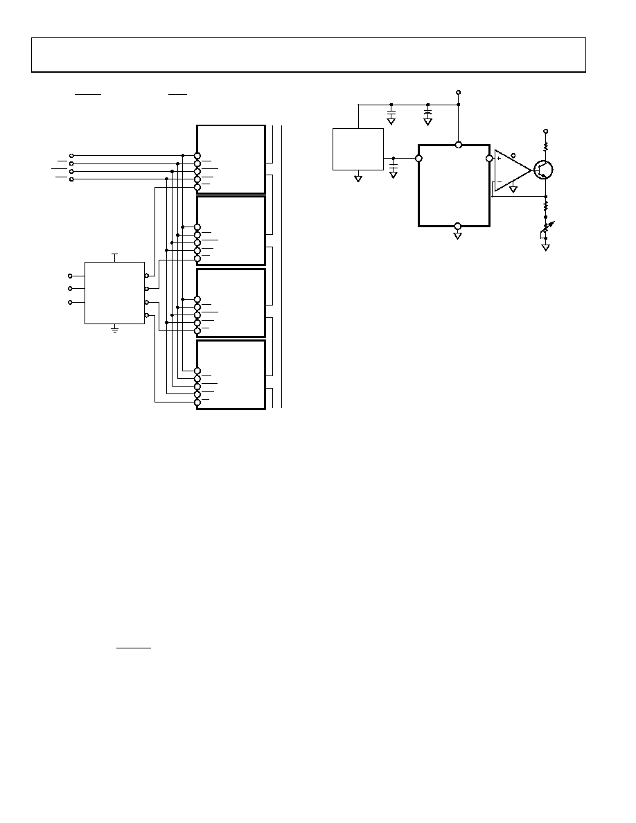
a system, all the DACs can be updated simultaneously using a
common LDAC line. A common CLR line can also be used to
reset all DAC outputs to zero.
ENABLE
CODED
ADDRESS
G1
A1
B1
VDD
VCC
74HC139
DGND
1Y0
1Y1
1Y2
1Y3
DATA
INPUTS
DAT
A
BUS
*AD5341 ONLY
LDAC
CLR
CS
HBEN*
AD5330/AD5331/
AD5340/AD5341
WR
LDAC
CLR
HBEN*
WR
DATA
INPUTS
LDAC
CLR
CS
HBEN*
AD5330/AD5331/
AD5340/AD5341
WR
DATA
INPUTS
LDAC
CLR
CS
HBEN*
AD5330/AD5331/
AD5340/AD5341
WR
DATA
INPUTS
LDAC
CLR
CS
HBEN*
AD5330/AD5331/
AD5340/AD5341
WR
06
85
2-
04
7
Figure 46. Decoding Multiple DAC Devices
PROGRAMMABLE CURRENT SOURCE
Figure 47 shows the AD5330/AD5331/AD5340/AD5341 used
as the control element of a programmable current source. In
this example, the full-scale current is set to 1 mA. The output
voltage from the DAC is applied across the current setting
resistor of 4.7 kΩ in series with the 470 Ω adjustment poten-
tiometer, which gives an adjustment of about ±5%. Suitable
transistors to place in the feedback loop of the amplifier include
the BC107 and the 2N3904, which enable the current source to
operate from a minimum VSOURCE of 6 V. The operating range is
determined by the operating characteristics of the transistor.
having rail-to-rail operation on their outputs. The current for
any digital input code and resistor value can be calculated as
follows:
mA
)
2
(
R
D
V
G
I
N
REF
×
=
where:
G is the gain of the buffer amplifier (1 or 2).
D is the digital equivalent of the digital input code.
N is the DAC resolution (8, 10, or 12 bits).
R is the sum of the resistor plus adjustment potentiometer
in kilo ohms.
AD5330/AD5331/
AD5340/AD5341
VDD = 5V
4.7k
5V
470
LOAD
VSOURCE
VREF
VDD
GND
VOUT
AD820/
OP295
+
0.1F
10F
0.1F
GND
EXT
REF
VOUT
VIN
AD780/REF192
WITH VDD = 5V
06
85
2-
048
Figure 47. Programmable Current Source
POWER SUPPLY BYPASSING AND GROUNDING
In any circuit where accuracy is important, careful consid-
eration of the power supply and ground return layout helps
to ensure the rated performance. The printed circuit board on
which the AD5330/AD5331/AD5340/AD5341 are mounted
should be designed so that the analog and digital sections are
separated and confined to certain areas of the board. If the
device is in a system where multiple devices require an AGND-
to-DGND connection, the connection should be made at one
point only. The star ground point should be established as
closely as possible to the device. The AD5330/AD5331/
AD5340/AD5341 should have ample supply bypassing of
10 μF in parallel with 0.1 μF on the supply located as close to
the package as possible, ideally right up against the device.
The 10 μF capacitors are the tantalum bead type. The 0.1 μF
capacitor should have low effective series resistance (ESR) and
effective series inductance (ESI), like the common ceramic
types that provide a low impedance path to ground at high
frequencies to handle transient currents due to internal logic
switching.
The power supply lines of the device should use as large a trace
as possible to provide low impedance paths and reduce the
effects of glitches on the power supply line. Fast switching
signals such as clocks should be shielded with digital ground
to avoid radiating noise to other parts of the board, and should
never be run near the reference inputs. Avoid crossover of
digital and analog signals. Traces on opposite sides of the board
should run at right angles to each other. This reduces the effects
of feedthrough through the board. A microstrip technique is by
far the best, but not always possible with a double-sided board.
In this technique, the component side of the board is dedicated to
the ground plane while signal traces are placed on the solder side.
相关PDF资料 |
PDF描述 |
|---|---|
| MS3120F22-21S | CONN RCPT 21POS WALL MNT W/SCKT |
| M83723/95G14076 | CONN PLUG 7POS STRAIGHT W/SCKT |
| MS3116F22-41SW | CONN PLUG 41POS STRAIGHT W/SCKT |
| MS3456KS14S-6S | CONN PLUG 6POS STRAIGHT W/SCKT |
| AD5312ARMZ | IC DAC 10BIT DUAL R-R 10-MSOP |
相关代理商/技术参数 |
参数描述 |
|---|---|
| AD5331BRUZ1 | 制造商:AD 制造商全称:Analog Devices 功能描述:2.5 V to 5.5 V, 115 ??A, Parallel Interface Single Voltage-Output 8-/10-/12-Bit DACs |
| AD5331BRUZ-REEL | 功能描述:IC DAC 10BIT SNGL VOUT 20-TSSOP RoHS:是 类别:集成电路 (IC) >> 数据采集 - 数模转换器 系列:- 产品培训模块:Data Converter Fundamentals DAC Architectures 设计资源:Unipolar, Precision DC Digital-to-Analog Conversion using AD5450/1/2/3 8-14-Bit DACs (CN0052) Precision, Bipolar, Configuration for AD5450/1/2/3 8-14bit Multiplying DACs (CN0053) AC Signal Processing Using AD5450/1/2/3 Current Output DACs (CN0054) Programmable Gain Element Using AD5450/1/2/3 Current Output DAC Family (CN0055) Single Supply Low Noise LED Current Source Driver Using a Current Output DAC in the Reverse Mode (CN0139) 标准包装:10,000 系列:- 设置时间:- 位数:12 数据接口:DSP,MICROWIRE?,QSPI?,串行,SPI? 转换器数目:1 电压电源:单电源 功率耗散(最大):- 工作温度:-40°C ~ 125°C 安装类型:表面贴装 封装/外壳:SOT-23-8 薄型,TSOT-23-8 供应商设备封装:TSOT-23-8 包装:带卷 (TR) 输出数目和类型:1 电流,单极;1 电流,双极 采样率(每秒):2.7M |
| AD5331BRUZ-REEL1 | 制造商:AD 制造商全称:Analog Devices 功能描述:2.5 V to 5.5 V, 115 ??A, Parallel Interface Single Voltage-Output 8-/10-/12-Bit DACs |
| AD5331BRUZ-REEL7 | 功能描述:IC DAC 10BIT SNGL VOUT 20-TSSOP RoHS:是 类别:集成电路 (IC) >> 数据采集 - 数模转换器 系列:- 产品培训模块:Data Converter Fundamentals DAC Architectures 设计资源:Unipolar, Precision DC Digital-to-Analog Conversion using AD5450/1/2/3 8-14-Bit DACs (CN0052) Precision, Bipolar, Configuration for AD5450/1/2/3 8-14bit Multiplying DACs (CN0053) AC Signal Processing Using AD5450/1/2/3 Current Output DACs (CN0054) Programmable Gain Element Using AD5450/1/2/3 Current Output DAC Family (CN0055) Single Supply Low Noise LED Current Source Driver Using a Current Output DAC in the Reverse Mode (CN0139) 标准包装:10,000 系列:- 设置时间:- 位数:12 数据接口:DSP,MICROWIRE?,QSPI?,串行,SPI? 转换器数目:1 电压电源:单电源 功率耗散(最大):- 工作温度:-40°C ~ 125°C 安装类型:表面贴装 封装/外壳:SOT-23-8 薄型,TSOT-23-8 供应商设备封装:TSOT-23-8 包装:带卷 (TR) 输出数目和类型:1 电流,单极;1 电流,双极 采样率(每秒):2.7M |
| AD5331BRUZ-REEL71 | 制造商:AD 制造商全称:Analog Devices 功能描述:2.5 V to 5.5 V, 115 ??A, Parallel Interface Single Voltage-Output 8-/10-/12-Bit DACs |
发布紧急采购,3分钟左右您将得到回复。