- 您现在的位置:买卖IC网 > PDF目录373878 > AD5339BRM-REEL7 (ANALOG DEVICES INC) 2.5 V to 5.5 V, 250 UA, 2-Wire Interface Dual-Voltage Output, 8-/10-/12-Bit DACs PDF资料下载
参数资料
| 型号: | AD5339BRM-REEL7 |
| 厂商: | ANALOG DEVICES INC |
| 元件分类: | DAC |
| 英文描述: | 2.5 V to 5.5 V, 250 UA, 2-Wire Interface Dual-Voltage Output, 8-/10-/12-Bit DACs |
| 中文描述: | SERIAL INPUT LOADING, 8 us SETTLING TIME, 12-BIT DAC, PDSO8 |
| 封装: | MO-187AA, MSOP-8 |
| 文件页数: | 15/24页 |
| 文件大小: | 654K |
| 代理商: | AD5339BRM-REEL7 |
AD5337/AD5338/AD5339
FUNCTIONAL DESCRIPTION
The AD5337/AD5338/AD5339 are dual resistor-string DACs
fabricated on a CMOS process with resolutions of 8, 10, and
12 bits, respectively. Each contains two output buffer amplifiers
and is written to via a 2-wire serial interface. The DACs operate
from single supplies of 2.5 V to 5.5 V, and the output buffer
amplifiers provide rail-to-rail output swing with a slew rate of
0.7 V/μs. The two DACs share a single reference input pin.
Each DAC has three programmable power-down modes that
allow the output amplifier to be configured with either a 1 k
load to ground, a 100 k load to ground, or as a high
impedance three-state output.
Rev. A | Page 15 of 24
DIGITAL-TO-ANALOG CONVERTER SECTION
The architecture of one DAC channel consists of a resistor-
string DAC followed by an output buffer amplifier. The voltage
at the REFIN pin provides the reference voltage for the DAC.
Figure 29 shows a block diagram of the DAC architecture.
Because the input coding to the DAC is straight binary, the ideal
output voltage is given by
N
REF
2
OUT
V
D
V
×
=
where:
D
is the decimal equivalent of the binary code, which is loaded
to the DAC register;
0–255 for AD5337 (8 bits)
0–1023 for AD5338 and AD5338-1 (10 bits)
0–4095 for AD5339 (12 bits)
N
is the DAC resolution
INPUT
REGISTER
REFIN
OUTPUT BUFFER
AMPLIFIER
V
OUT
A
RESISTOR
STRING
DAC
REGISTER
0
Figure 29. DAC Channel Architecture
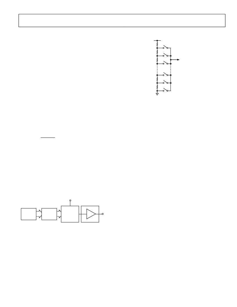
RESISTOR STRING
The resistor string portion is shown in Figure 30. It is simply a
string of resistors, each of value R. The digital code loaded to
the DAC register determines the node at which the voltage is
tapped off and fed into the output amplifier. The voltage is
tapped off by closing one of the switches that connects the
string to the amplifier. Because the DAC comprises a string
of resistors, it is guaranteed to be monotonic.
R
R
R
R
R
TO OUTPUT
AMPLIFIER
0
Figure 30. Resistor String
DAC REFERENCE INPUTS
There is a single reference input pin for the two DACs. The
reference input is unbuffered. The user can have a reference
voltage as low as 0.25 V and as high as V
DD
, since there is no
restriction due to headroom and foot room of any reference
amplifier.
It is recommended to use a buffered reference in the external
circuit, for example, REF192. The input impedance is typically
45 k.
OUTPUT AMPLIFIER
The output buffer amplifier is capable of generating rail-to-rail
voltages on its output, which gives an output range of 0 V to
V
DD
when the reference is V
DD
. The amplifier is capable of
driving a load of 2 k to GND or V
DD
in parallel with 500 pF to
GND or V
DD
. The source and sink capabilities of the output
amplifier can be seen in the plot in Figure 16.
The slew rate is 0.7 V/μs with a half-scale settling time to
±0.5 LSB (at 8 bits) of 6 μs.
POWER-ON RESET
The AD5337/AD5338/AD5339 power on in a defined state via a
power-on reset function. The power-on state is normal
operation, with output voltage set to 0 V.
Both input and DAC registers are filled with zeros until a valid
write sequence is made to the device. This is particularly useful
in applications where it is important to know the state of the
DAC outputs while the device is powering on.
SERIAL INTERFACE
The AD5337/AD5338/AD5339 are controlled via an I
2
C-
compatible serial bus. The DACs are connected to this bus as
slave devices—that is, no clock is generated by the AD5337/
AD5338/AD5339 DACs. This interface is SMBus-compatible at
V
DD
< 3.6 V.
相关PDF资料 |
PDF描述 |
|---|---|
| AD534K | Dual 14-bit 105MSPS ADC with serialized LVDS output 48-VQFN -40 to 85 |
| AD534KD | Dual 14-bit 125MSPS ADC with serialized LVDS output 48-VQFN -40 to 85 |
| AD534KH | Dual 14-bit 125MSPS ADC with serialized LVDS output 48-VQFN -40 to 85 |
| AD534L | Dual 14-bit 125MSPS ADC with serialized LVDS output 48-VQFN -40 to 85 |
| AD534LD | Dual 14-bit 125MSPS ADC with serialized LVDS output 48-VQFN -40 to 85 |
相关代理商/技术参数 |
参数描述 |
|---|---|
| AD5339BRMZ | 功能描述:IC DAC 12BIT DUAL 2-WIRE 8-MSOP RoHS:是 类别:集成电路 (IC) >> 数据采集 - 数模转换器 系列:- 标准包装:1 系列:- 设置时间:4.5µs 位数:12 数据接口:串行,SPI? 转换器数目:1 电压电源:单电源 功率耗散(最大):- 工作温度:-40°C ~ 125°C 安装类型:表面贴装 封装/外壳:8-SOIC(0.154",3.90mm 宽) 供应商设备封装:8-SOICN 包装:剪切带 (CT) 输出数目和类型:1 电压,单极;1 电压,双极 采样率(每秒):* 其它名称:MCP4921T-E/SNCTMCP4921T-E/SNRCTMCP4921T-E/SNRCT-ND |
| AD5339BRMZ-REEL | 功能描述:IC DAC 12BIT DUAL 2-WIRE 8-MSOP RoHS:是 类别:集成电路 (IC) >> 数据采集 - 数模转换器 系列:- 标准包装:47 系列:- 设置时间:2µs 位数:14 数据接口:并联 转换器数目:1 电压电源:单电源 功率耗散(最大):55µW 工作温度:-40°C ~ 85°C 安装类型:表面贴装 封装/外壳:28-SSOP(0.209",5.30mm 宽) 供应商设备封装:28-SSOP 包装:管件 输出数目和类型:1 电流,单极;1 电流,双极 采样率(每秒):* |
| AD5339BRMZ-REEL7 | 功能描述:IC DAC 12BIT DUAL 2-WIRE 8-MSOP RoHS:是 类别:集成电路 (IC) >> 数据采集 - 数模转换器 系列:- 标准包装:47 系列:- 设置时间:2µs 位数:14 数据接口:并联 转换器数目:1 电压电源:单电源 功率耗散(最大):55µW 工作温度:-40°C ~ 85°C 安装类型:表面贴装 封装/外壳:28-SSOP(0.209",5.30mm 宽) 供应商设备封装:28-SSOP 包装:管件 输出数目和类型:1 电流,单极;1 电流,双极 采样率(每秒):* |
| AD533JD | 制造商:Rochester Electronics LLC 功能描述:- Bulk |
| AD533JH | 制造商:Rochester Electronics LLC 功能描述:- Bulk |
发布紧急采购,3分钟左右您将得到回复。