- 您现在的位置:买卖IC网 > PDF目录373878 > AD5339BRM-REEL7 (ANALOG DEVICES INC) 2.5 V to 5.5 V, 250 UA, 2-Wire Interface Dual-Voltage Output, 8-/10-/12-Bit DACs PDF资料下载
参数资料
| 型号: | AD5339BRM-REEL7 |
| 厂商: | ANALOG DEVICES INC |
| 元件分类: | DAC |
| 英文描述: | 2.5 V to 5.5 V, 250 UA, 2-Wire Interface Dual-Voltage Output, 8-/10-/12-Bit DACs |
| 中文描述: | SERIAL INPUT LOADING, 8 us SETTLING TIME, 12-BIT DAC, PDSO8 |
| 封装: | MO-187AA, MSOP-8 |
| 文件页数: | 16/24页 |
| 文件大小: | 654K |
| 代理商: | AD5339BRM-REEL7 |
AD5337/AD5338/AD5339
The AD5337/AD5338/AD5339 have a 7-bit slave address. The
six MSBs are 000110, and the LSB is determined by the state of
the A0 pin. The facility of making hardwired changes to A0
allows the use of one or two of these devices on one bus. The
AD5338-1 has a unique 7-bit slave address. The six MSBs are
010001, and the LSB is again determined by the state of the A0
pin. Using a combination of AD5338 and AD5338-1 allows the
user to accommodate four of these dual 10-bit devices (eight
channels) on the same bus.
Rev. A | Page 16 of 24
The 2-wire serial bus protocol operates as follows:
1.
The master initiates data transfer by establishing a start
condition when a high-to-low transition on the SDA line
occurs while SCL is high. The following byte is the address
byte, which consists of the 7-bit slave address, followed by
an R/W bit. (This bit determines whether data is read from
or written to the slave device.)
The slave with the address corresponding to the transmitted
address responds by pulling SDA low during the ninth
clock pulse (this is termed the acknowledge bit). At this
stage, all other devices on the bus remain idle while the
selected device waits for data to be written to or read from
its shift register.
2.
Data is transmitted over the serial bus in sequences of nine
clock pulses (eight data bits, followed by an acknowledge
bit). The transitions on the SDA line must occur during the
low period of SCL and remain stable during the high period
of SCL.
3.
When all data bits have been read from or written to, a stop
condition is established. In write mode, the master pulls
the SDA line high during the 10th clock pulse to establish a
stop condition. In read mode, the master issues a No
Acknowledge for the ninth clock pulse, that is, the SDA
line remains high. The master then brings the SDA line low
before the 10th clock pulse and high during the 10th clock
pulse to establish a stop condition.
Read/Write Sequence
For the AD5337/AD5338/AD5339, all write access sequences
and most read sequences begin with the device address (with
R/W = 0), followed by the pointer byte. This pointer byte specifies
the data format and determines which DAC is being accessed in
the subsequent read/write operation. See Figure 31. In a write
operation, the data follows immediately. In a read operation, the
address is resent with R/W = 1, and then the data is read back.
However, it is also possible to perform a read operation by
sending only the address with R/W = 1. The previously loaded
pointer settings are then used for the read back operation. See
Figure 32 for a graphical explanation of the interface.
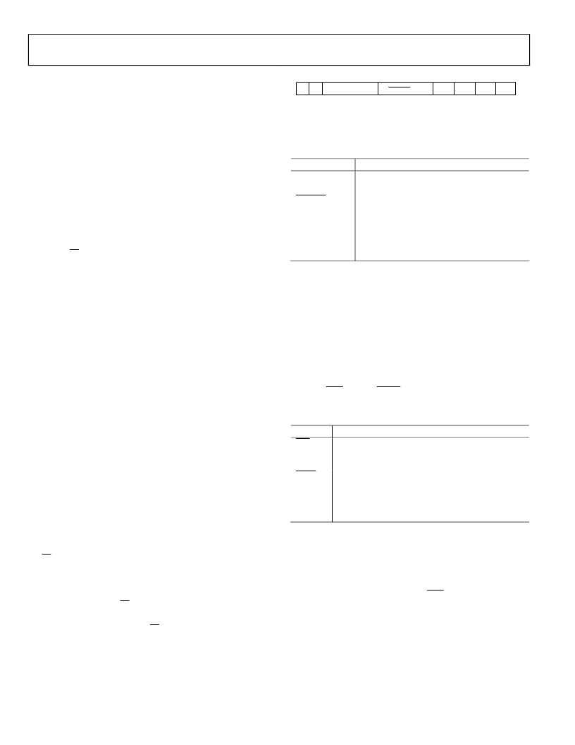
0
0
X
X
LSB
MSB
0
DACB DACA
DOUBLE = 0
0
Figure 31. Pointer Byte
The following table explains the individual bits that make up
the pointer byte.
Table 6. Pointer Byte Bits
Pointer
Byte Bits
X
Don’t care bits.
0: Bit set to 0.
DOUBLE
0: Data write and readback are done as 2-byte
write/read sequences.
0: Bit set to 0.
0: Bit set to 0.
DACB
1: The following data bytes are for DAC B.
DACA
1: The following data bytes are for DAC A.
Input Shift Register
The input shift register is 16 bits wide. Data is loaded into the
device as two data bytes on the serial data line, SDA, under the
control of the serial clock input, SCL. The timing diagram for
this operation is shown in Figure 2. The two data bytes consist
of four control bits followed by 8, 10, or 12 bits of DAC data,
depending on the device type. The first two bits loaded are PD1
and PD0 bits that control the mode of operation of the device.
See the Power-Down Modes section for a complete description.
Bit 13 is CLR, Bit 12 is LDAC, and the remaining bits are left-
justified DAC data bits, starting with the MSB. See Figure 32.
Table 7. Input Shift Register
Register
Setting and Result
CLR
0: All DAC registers and input registers are filled with
0s on completion of the write sequence.
1: Normal operation.
LDAC
0: The two DAC registers and therefore all DAC
outputs simultaneously updated on completion of
the write sequence.
1: Addressed input register only is updated. There is
no change in the contents of the DAC registers.
Default Read Back Condition
All pointer byte bits power-up to 0. Therefore, if the user
initiates a readback without writing to the pointer byte first, no
single DAC channel has been specified. In this case, the default
readback bits are all 0, except for the CLR bit, which is 1.
Multiple-DAC Write Sequence
Because there are individual bits in the pointer byte for each
DAC, it is possible to write the same data and control bits to two
DACs simultaneously by setting the relevant bits to 1.
相关PDF资料 |
PDF描述 |
|---|---|
| AD534K | Dual 14-bit 105MSPS ADC with serialized LVDS output 48-VQFN -40 to 85 |
| AD534KD | Dual 14-bit 125MSPS ADC with serialized LVDS output 48-VQFN -40 to 85 |
| AD534KH | Dual 14-bit 125MSPS ADC with serialized LVDS output 48-VQFN -40 to 85 |
| AD534L | Dual 14-bit 125MSPS ADC with serialized LVDS output 48-VQFN -40 to 85 |
| AD534LD | Dual 14-bit 125MSPS ADC with serialized LVDS output 48-VQFN -40 to 85 |
相关代理商/技术参数 |
参数描述 |
|---|---|
| AD5339BRMZ | 功能描述:IC DAC 12BIT DUAL 2-WIRE 8-MSOP RoHS:是 类别:集成电路 (IC) >> 数据采集 - 数模转换器 系列:- 标准包装:1 系列:- 设置时间:4.5µs 位数:12 数据接口:串行,SPI? 转换器数目:1 电压电源:单电源 功率耗散(最大):- 工作温度:-40°C ~ 125°C 安装类型:表面贴装 封装/外壳:8-SOIC(0.154",3.90mm 宽) 供应商设备封装:8-SOICN 包装:剪切带 (CT) 输出数目和类型:1 电压,单极;1 电压,双极 采样率(每秒):* 其它名称:MCP4921T-E/SNCTMCP4921T-E/SNRCTMCP4921T-E/SNRCT-ND |
| AD5339BRMZ-REEL | 功能描述:IC DAC 12BIT DUAL 2-WIRE 8-MSOP RoHS:是 类别:集成电路 (IC) >> 数据采集 - 数模转换器 系列:- 标准包装:47 系列:- 设置时间:2µs 位数:14 数据接口:并联 转换器数目:1 电压电源:单电源 功率耗散(最大):55µW 工作温度:-40°C ~ 85°C 安装类型:表面贴装 封装/外壳:28-SSOP(0.209",5.30mm 宽) 供应商设备封装:28-SSOP 包装:管件 输出数目和类型:1 电流,单极;1 电流,双极 采样率(每秒):* |
| AD5339BRMZ-REEL7 | 功能描述:IC DAC 12BIT DUAL 2-WIRE 8-MSOP RoHS:是 类别:集成电路 (IC) >> 数据采集 - 数模转换器 系列:- 标准包装:47 系列:- 设置时间:2µs 位数:14 数据接口:并联 转换器数目:1 电压电源:单电源 功率耗散(最大):55µW 工作温度:-40°C ~ 85°C 安装类型:表面贴装 封装/外壳:28-SSOP(0.209",5.30mm 宽) 供应商设备封装:28-SSOP 包装:管件 输出数目和类型:1 电流,单极;1 电流,双极 采样率(每秒):* |
| AD533JD | 制造商:Rochester Electronics LLC 功能描述:- Bulk |
| AD533JH | 制造商:Rochester Electronics LLC 功能描述:- Bulk |
发布紧急采购,3分钟左右您将得到回复。